RFSi® wafers – High Resistivity line for RF
Okmetic’s comprehensive line of high resistivity RFSi® silicon wafers provides an optimal platform for the manufacture of RF filters and devices. Our high resistivity RFSi® wafers improve RF device performance, Total Cost of Ownership and enable more ambitious designs.
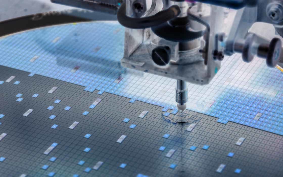
Okmetic is the leading supplier of advanced silicon wafers for the RF market and the company has had strong focus on RF wafer solutions for years. Okmetic has delivered over 2 million wafers for the RF market and the deliveries doubled in 2021 compared to 2020. Okmetic high resistivity RFSi® wafers provide and optimal platform for BAW and TF-SAW filters, IPD devices, power amplifiers, RFIC applications and silicon interposers. These filters and devices are used in smartphones and communication devices to enable faster data transfer and greater capacity propelled by 5G and 4G technologies.
RFSi® wafers provide and optimal platform for RF filters and devices used in smartphones and communication devices to enable faster data transfer.
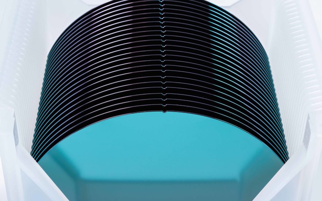
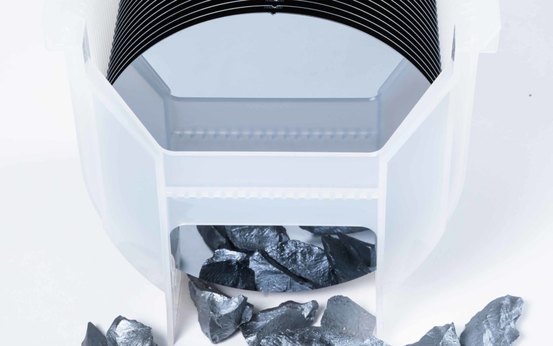
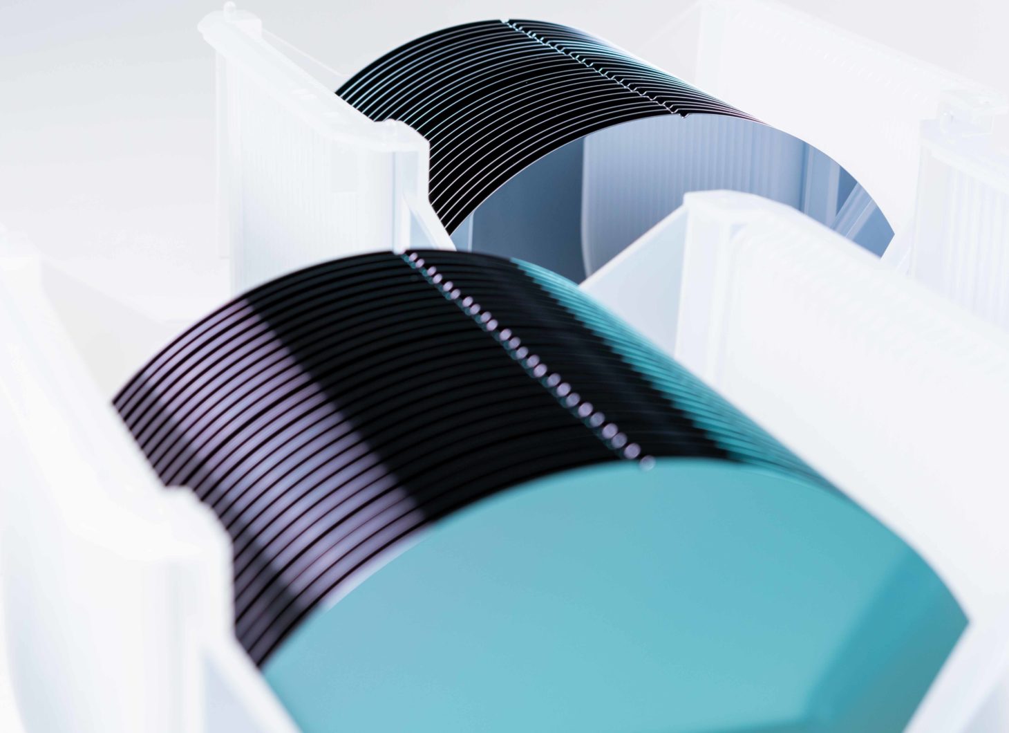
Okmetic’s RFSi® portfolio is a line of specialty wafers combining up to over 10,000 ohm-centimeters of bulk resistivities with advanced surface engineering. These wafers are manufactured by using Okmetic’s trademark Advanced Magnetic Czochralski (A-MCz®) crystal growth method, trap-rich layer and advanced planarization technology. The very high and stable resistivity of Okmetic RFSi® wafers enable superior RF filter and device performance, lower Total Cost of Ownership and more ambitious device designs.
Comprehensive line of High Resistivity RFSi® wafers
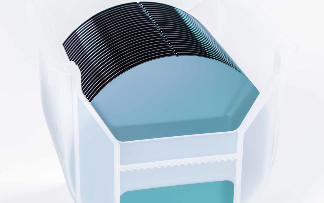
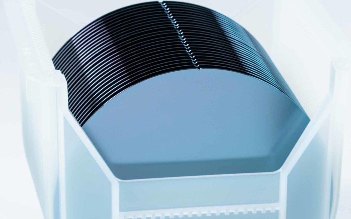
Okmetic has comprehensive RFSi® wafer line consisting of specialty wafers reaching up to over 10,000 ohm-centimeters of bulk resistivities. Resistivity, Crystal Orientation, Oxygen content, and Thickness can be customized to match your product or package needs. Okmetic provides wide range of wafer thicknesses from 380 to 1,150 μm. Our RF customers find the thinner options very attractive in packaging designs whereas in mixed metal lattices like GaN epi layers, they enjoy the benefits of the thicker wafers to offset the extreme stresses. Our sales and technical support are happy to help finding an optimal solution, customized for your needs.
Okmetic’s RFSi® wafer line consist of the following products:
- Engineered Ultra High Resistivity wafers
- Engineered High Resistivity wafers with trap-rich layer
- UF-RFSi® wafers – Ultra Flat High Resistivity
- High Resistivity wafers
- High Resistivity BSOI wafers including C-SOI® wafers
- RF GaN Substrate wafers for GaN-on-Si applications
Typical RFSi® wafer specifications
| Growth method | MCz, A-MCz® |
| Diameter | 150 mm, 200 mm |
| Crystal orientation | <100>, <111> |
| N type dopants | Phosphorus |
| P type dopants | Boron |
| Resistivity | Up to > 10,000 Ohm-cm* *Resistivity range varies by dopant and orientation |
| Oxygen | Typically ≤ 5 ppma or ≤ 10 ppma (ASTM F121-83). Can be optimized to Customer process. |
| SSP (etched backside) wafer thickness | 150 mm: 400 to 1,150 µm; 200 mm: 550 to 1,150 µm* *Other thicknesses possible with certain limitations |
| DSP (polished backside) wafer thickness | 150 mm: 380 to >1,150 µm; 200 mm: 380 to 1,150 µm* *Other thicknesses possible with certain limitations |
RFSi® wafer benefits
- Record low insertion losses
- High Q-values
- Linear 2nd harmonics characteristics over temperature
- New design option for TF-SAW utilizing the UF-RFSi® wafer
- High Resistivity wafer characteristics combined to Cavity SOI offer readily made suspended low loss structures.
A-MCz® crystal growth method vs FZ method
- Cost benefit over high resistivity FZ, especially in 200mm
- Availability in 111 orientation
- Optimized Oi range to increase wafer strength at customer process. Less prone to slip and breakage.
- Engineered A-MCz® wafer option adds value through the trap-rich layer that Okmetic helps match with customer’s specific process/product.