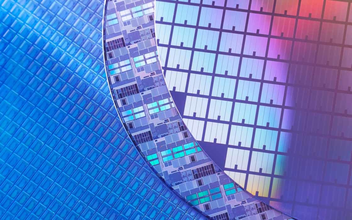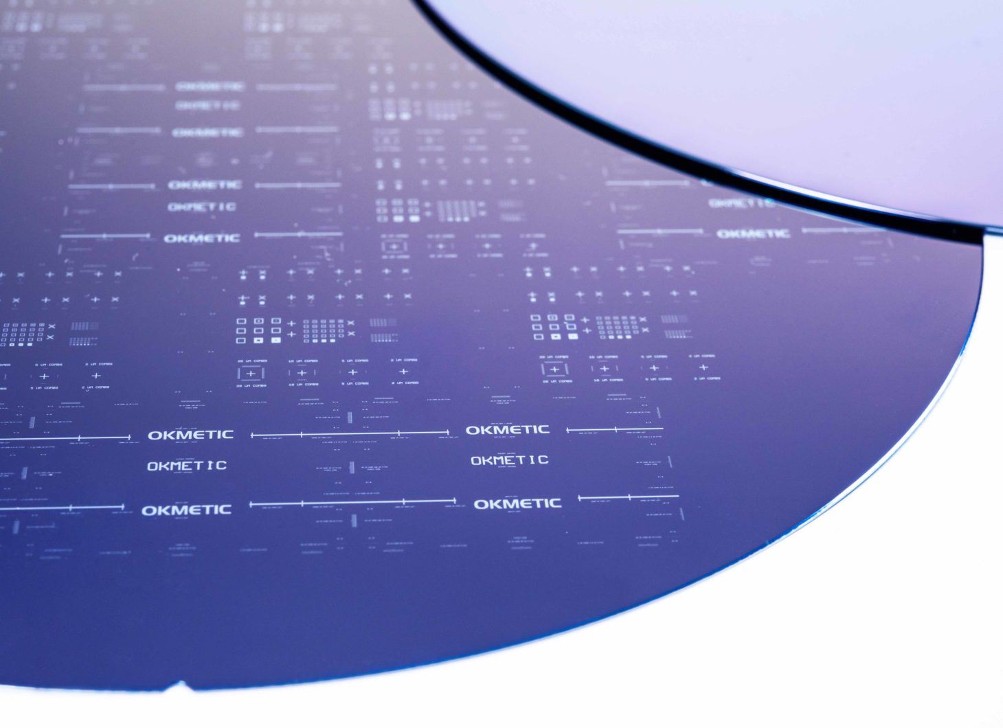
C-SOI® wafers – Cavity SOI
Okmetic C-SOI® is a bonded SOI wafer that has built-in sealed cavities on the handle wafer or on the buried oxide. C-SOI® represents the most advanced silicon wafer technology and can be considered as a partially built sensor or electronic device rather than just a wafer. The benefits are unparalleled: more streamlined and cost-effective device manufacturing and more ambitious device designs.
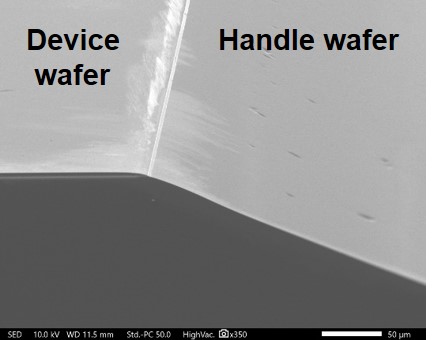
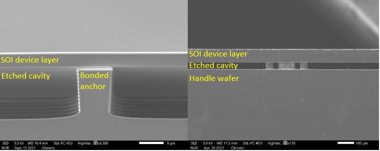
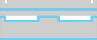
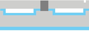
Okmetic C-SOI® is a bonded Cavity Silicon On Insulator wafer, which has built-in sealed cavity patterning etched on the bottom handle wafer or on the buried oxide (BOX) layer before bonding and thinning the top silicon wafer acting as a device layer. Okmetic can supply wafers that have customer alignment marks on top of the device layer to convey information on exact cavity location. This ensures smooth integration of Okmetic and customer processes. The cavities are used to simplify device manufacturing and they can be integrated into the active, passive or structural elements of the device. This makes it possible to process more complex and developed structures than would be possible with the standard BSOI wafers. The cavities can also be used for integrations of IC and MEMS processes further increasing the usage possibilities. Okmetic manufactures these wafers in line with identical quality and cleanliness standards as standard bulk silicon wafers.
C-SOI® wafer is more like a partially built sensor than just a wafer, which makes it an optimal platform for MEMS
C-SOI® wafers are more than just wafers, in fact they can be better described as partially built sensors or electronic components as their advanced technology enables more streamlined MEMS production process. This is one reason why their usage as a platform for MEMS and sensor devices has surged rapidly during the past few years after steady growth during the past decade.
Required membrane thickness varies across applications
Okmetic’s high-technology cavity SOI process enables the manufacture of extremely thin and thick membranes, which expands the variety of device design and processing possibilities. Okmetic Cavity SOI wafers with thin membranes are widely used e.g. for pressure sensors, silicon speakers and ultrasonic transducers like PMUT and CMUT’s. Cavity SOI wafers with thicker membranes offer significant benefits for devices such as inertial sensors (gyroscopes, accelerometers, IMUs), micromirrors and other optical devices (like optical switches etc.). Depending on the design, either thin or thick membranes can be used for microfluidic devices like inkjet heads, timing devices and other resonators and IC and MEMS process integrations. In addition, SOI wafers usage is also expanding into RF devices, for the needs of which Okmetic has developed High Resistivity BSOI and C-SOI® wafers.
C-SOI® specifications
The tables below give some guidelines on Okmetic C-SOI® wafer specifications. Our C-SOI® wafers are always customized solutions, so please contact our sales and technical support for more detailed information.
| C-SOI® wafer diameter | 150 mm, 200 mm |
Device layer specifications
| Growth method | Cz, MCz, A-MCz® |
| Crystal orientation | <100>, <110>, <111> |
| N type dopants | Antimony, Phosphorus |
| P type dopants | Boron |
| Resistivity | From <0.001 to >7,000 Ohm-cm* *Resistivity range varies by dopant and orientation |
| Device layer / membrane thickness | From 2 μm to >200 μm |
| Device layer / membrane thickness tolerance | Typically ±0.5 μm, down to ±0.2 μm with EC-SOI |
Buried oxide (BOX) specifications
| Type | Thermal oxide grown on handle or device wafer or both |
| Thickness | From 0.3 μm to 4 μm, typically between 0.5 μm and 2 μm |
Handle wafer specifications
| Growth method | Cz, MCz, A-MCz® |
| Crystal orientation | <100>, <110>, <111> |
| N type dopants | Antimony, Phosphorus |
| P type dopants | Boron |
| Resistivity | From <0.001 to >7,000 Ohm-cm* *Resistivity range varies by dopant and orientation |
| Handle wafer thickness | 200 mm: 300 μm to 950 μm, typically 725 μm 150 mm: 300 μm to 950 μm, typically 380 μm |
| Handle wafer thickness tolerance | ±5 μm |
| Back surface | Polished or etched with oxide |
Cavity specifications
| Cavity location | Handle wafer or device layer, or buried oxide |
| Cavity depth (in silicon) | 2 – 500 µm |
| Minimum CD | 2 µm |
| Max cavity span length vs. membrane thickness | <40:1 µm with standard C-SOI® process |
Front surface alignment marks
| Alignment accuracy, buried cavity to front surface alignment marks | ±1 µm |
| Mark design | Customer tool specific |
C-SOI® wafers optimize MEMS manufacturing process
C-SOI® wafers have many benefits compared to bulk silicon micro-machining and even traditional SOI technology: more cost-effective and streamlined MEMS manufacturing process and more complex, advanced and better-performing devices.
C-SOI® wafer is an advanced solution with multiple benefits:
- Reduced device size and cost
- Superior device performance and precision
- Increased device reliability
- More advanced device designs
- Optimized device manufacturing process resulting to lower costs and faster time to market
More advanced designs and superior performance and precision
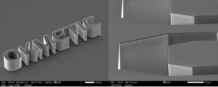
Okmetic’s patterning and etching process has best-in-class etching uniformity. Okmetic’s ability to produce C-SOI® wafers with extremely thin and thick membranes, well-defined horizontal dimensions and flexibility to adjust the gap between released structure and the substrate enable manufacture of more advanced device designs. Cavity SOI wafers also enable the optimization of efficiency and electrical properties through minimization of parasitic capacitances. In addition, process optimization advantages can be gained through integrated backside packaging and hermetic sealing.
Customized Cavity SOI solutions with shorter cycle time and better quality
C-SOI® wafers are customized to match customer device design and process seamlessly. Customer device design is taken into account throughout the manufacturing process, starting from the crystal growth phase.
Holistic approach to C-SOI®wafer design and processing increase quality and reliability of wafers and optimize the MEMS production process
Okmetic has been producing Cavity SOI wafers since 2005. Okmetic’s patterning and DRIE cavity etching is a fully in-house process, which reduces the Cavity SOI wafer cycle time significantly as there is no need to ship wafers to customers for cavity etching and then back to Okmetic for bonding. But most importantly, this kind of holistic approach to C-SOI® wafer design and processing has increased the quality and reliability of wafers and helped optimize the MEMS production process. Read more about Okmetic’s patterning and cavity etching process and wafer tailoring.
Cost-effectiveness over bulk silicon MEMS and traditional SOI technology
C-SOI® wafers offer extremely cost-effective solution over bulk silicon micromachining and even BSOI wafers. As an example, when manufacturing a pressure sensor on 400 µm thick wafer the cost per chip can be reduced by 50% compared to bulk silicon micromachining and 25% compared to BSOI wafers. This is because the patterning, etching and bonding costs are included in the C-SOI® wafer price and the device size is smaller when using the more advanced C-SOI® wafer platform.
C-SOI® variations for specialized needs
EC-SOI wafer
Okmetic EC-SOI combines state-of-the-art silicon technologies such as highly uniform E-SOI® wafer with embedded cavity structures of C-SOI® wafer. EC-SOI wafer is a new kind of enabling substrate, which opens up new possibilities for advanced MEMS devices such as silicon photonic integrated circuits (PICs) and ultrasonic transducers, with PMUTs and CMUTs.
Double C-SOI® wafer
Okmetic Double C-SOI® wafer combines two device and buried oxide layers with cavities on handle wafer. This combination has shown to add value for MEMS and photonics devices.
C-SOI® wafer with patterned device layer

C-SOI® wafer’s cavities are patterned on the device layer instead of the handle wafer. Read more about our patterning process.
C-SOI® wafer with poly via
C-SOI® wafer with through Buried Oxide via form electrical non-isolated contact between device and handle wafer. This can be used for device layer grounding.