Skip to content
To front page
  • Silicon Wafers
    • MEMS Wafer Line
      • MEMS SSP and DSP Wafers
      • Selecting the ideal wafer for MEMS devices: Balancing cost, performance, and manufacturing efficiency
    • RFSi® Wafer Line – High Resistivity for RF
      • High Resistivity Wafers
      • Engineered High Resistivity Wafers with Trap-Rich Layer
      • Engineered Ultra High Resistivity wafers
      • UF-RFSi® – Ultra Flat High Resistivity Wafers
      • High Resistivity BSOI Wafers
      • RF GaN Substrate wafers
    • Power Wafer Line
      • Power Management SOI wafers
      • Power GaN Substrate wafers (Si and SOI) 
      • Discrete Power Device wafers 
    • SOI Wafers – Silicon-On-Insulator Line
      • BSOI Wafers – Bonded SOI
      • C-SOI® Wafers – Cavity SOI
      • E-SOI® Wafers – Enhanced SOI
      • Terrace Free SOI wafers
    • Patterned Wafers – DRIE and Lithography
    • TSV Wafers – Through Silicon Via
    • DSP Wafers – Double Side Polished
    • SSP Wafers – Single Side Polished
    • Customized Wafers and Prototyping
    • Production and Capacity Expansion 
    • Supplier Awards and Collaboration Projects
  • Applications
    • MEMS and Sensors
    • RF Filters and Devices
    • Power Devices
  • Quality and Responsibility
    • Quality
      • Quality Policy
      • Quality Tools
        • Artificial Intelligence at Okmetic
        • 5S at Okmetic
    • Sustainability
      • Responsibility for Personnel
      • Responsibility for Safety and Health
      • Responsibility for Environment
      • Business Ethics
      • Managing Responsibility
      • Reports on Responsibility
    • Certificates
  • Work with Us
    • Production Experts
    • Semiconductor Professionals
    • Students
    • Maintenance professional
    • Technical professionals
    • Sales and technical support
    • Open Positions
  • About Okmetic
    • Company
    • Strategy and Values
    • Executive Management Group
    • Investments
    • Research and Development Work
    • Tale of a Silicon Wafer
    • The History of Okmetic
    • News & Insights
    • Contact Us
  • English
    • Suomi
    • 日本語
    • 中文 (中国)

Happy Lunar New Year 2023

News+1/20/2023
Okmetic+About Okmetic+News & insights+Happy Lunar New Year 2023

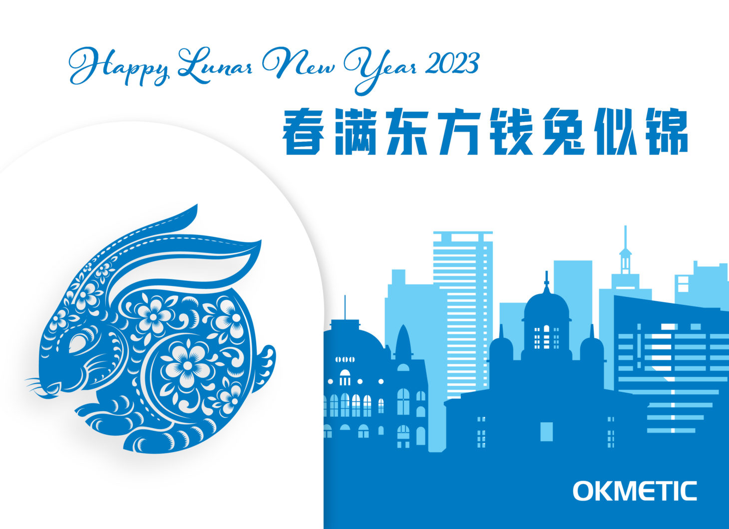
It’s time to bid farewell to the Year of the Tiger. Let’s welcome the new Year of the Rabbit! Okmetic wishes everyone a bright future and for all your wishes to be fulfilled!

Share page

Share on LinkedIn Share on Facebook WeChat YouTube

News & insights

PCIM sensors+test banner

Okmetic attending PCIM Europe and SENSOR+TEST

Learn more

The Sustainability Report for 2024 has been published 

Learn more
Mems Engineer Forum banner

Okmetic participating in MEMS Engineer Forum

Learn more

Okmetic achieved the highest Platinum level in a sustainability audit

Learn more

Okmetic Inc. President Reed gave a speech about substrates for GaN-on-Si and GaN-on-SOI at CMC Conference

Learn more
More news & insights
  • Silicon Wafers
    • Column
      • SOI Wafers – Silicon-On-Insulator Line
      • Patterned Wafers – DRIE and Lithography
      • TSV Wafers – Through Silicon Via
    • Column
      • RFSi® Wafers – High Resistivity Line for RF
      • SSP Wafers – Single Side Polished
      • DSP Wafers – Double Side Polished
    • Column
      • Power wafer line
      • Customized Wafers and Prototyping
      • Production and Subcontracting
To front page
  • About Okmetic
  • Contact Us
  • Applications
  • Quality and Responsibility
  • Work with Us
  • Privacy Policy and Terms of Use
  • Safety Data Sheet
LinkedIn YouTube WeChat Facebook