High Resistivity wafers
Okmetic High Resistivity SSP and DSP wafers combining low Oi and very high and stable resistivity enable improved electrical performance and reduced insertion losses of RF filters and devices.
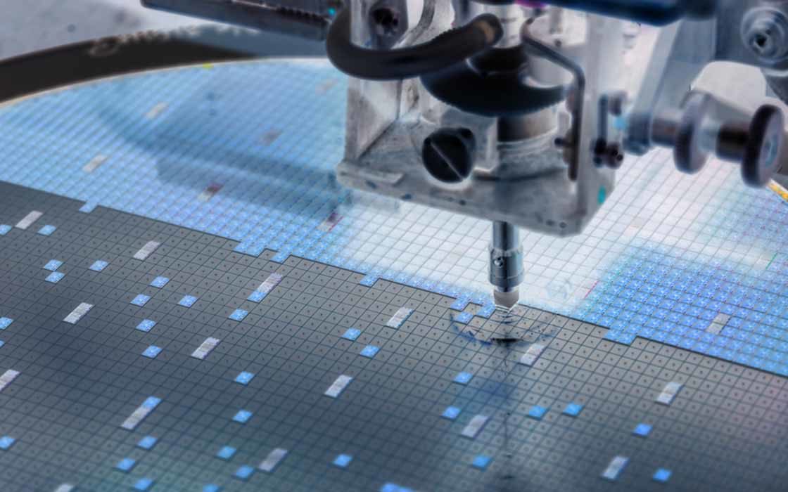
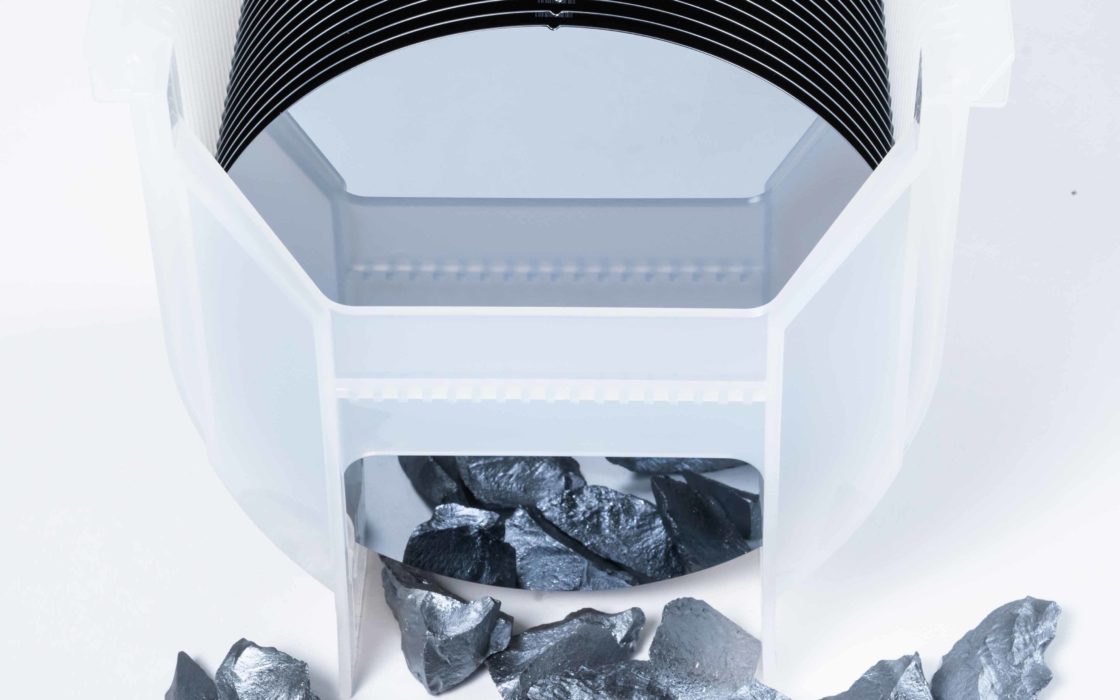
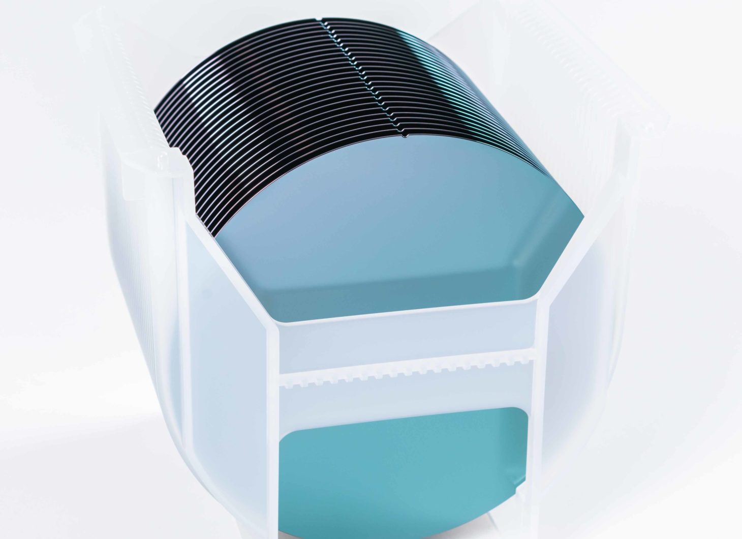
Okmetic High Resistivity silicon wafers are manufactured with Advanced Magnetic Czochralski (A-MCz®) crystal growth method and they combine low Oi and up to > 7,000 Ohm-cm resistivity. The High Resistivity wafers provide very high and stable resistivity, good electrical performance as well as reduced insertion losses.
Very high and stable resistivity, good electrical performance and reduced insertion losses
Okmetic High Resistivity silicon wafers are a good match for the needs of BAW SMR, FBAR and XBAR, SAW filter, IPD, silicon interposer and RFIC and quantum device applications. In case RF manufacturers are looking for even higher performance and record-low losses, Okmetic Engineered High Resistivity wafers with added trap-rich layer or Engineered Ultra High Resistivity wafers will help achieve these things.
High Resistivity wafer benefits:
- High, stable resisitivity
- Good electrical performance
- Reduced insertion losses
- Reduced characteristic stress and bow, mechanically stronger wafers
High resistivity with customized wafer parameters
Okmetic High Resistivity wafers are optimized, A-MCz® silicon wafers with low Oi and up to > 7,000 Ohm-cm resistivity. In addition to resistivities also other wafer parameters can be adjusted. The High Resistivity wafer selection includes 150 to 200 mm SSP and DSP silicon wafers doped with either Boron or Phosphorus. Crystal orientations include <100> and <111> and thicknesses range from 380 to >1,150 µm. The thin High Resistivity wafers enable more economical device integration in Wafer Level Packaging of silicon interposers. Also TSV (Through Silicon Vias) can be incorporated to them to further enhance the vertical packaging options.
High Resistivity wafer specifications
| Growth method | MCz, A-MCz® |
| Diameter | 150 mm, 200 mm |
| Crystal orientation | <100>, <111> |
| N type dopants | Phosphorus |
| P type dopants | Boron |
| Resistivity | Up to >7,000 Ohm-cm* *Resistivity range varies by dopant and orientation |
| Oxygen | Typically ≤5 ppma or ≤10 ppma (ASTM F121-83). Can be optimized to Customer process. |
| SSP (etched backside) wafer thickness | 200 mm: 550 to 1,150 µm* 150 mm: 400 to 1,150 µm *Other thicknesses possible with certain limitations |
| DSP (polished backside) wafer thickness | 200 mm: 380 to 1,150 µm* 150 mm: 380 to >1,150 µm *Other thicknesses possible with certain limitations |
Replace FZ substrates with a more robust and cost-effective solution
Okmetic High Resistivity RFSi® wafers are manufactured with the Advanced Magnetic Czochralski (A-MCz®) method. They provide a superior alternative to High Resistivity silicon wafers manufactured with the FZ (Float Zone) method. Lower Total Cost of Ownership is achieved through lower purchase prices, higher production volume and availability, better performance, improved integration possibilities, and lower fab handling costs. The High Resistivity MCz wafers are mechanically stronger and less vulnerable to thermal stress, thereby reducing dislocations, warp, fractures, and the associated fab and assembly wafer yield losses.
See all 150-200 mm silicon wafers