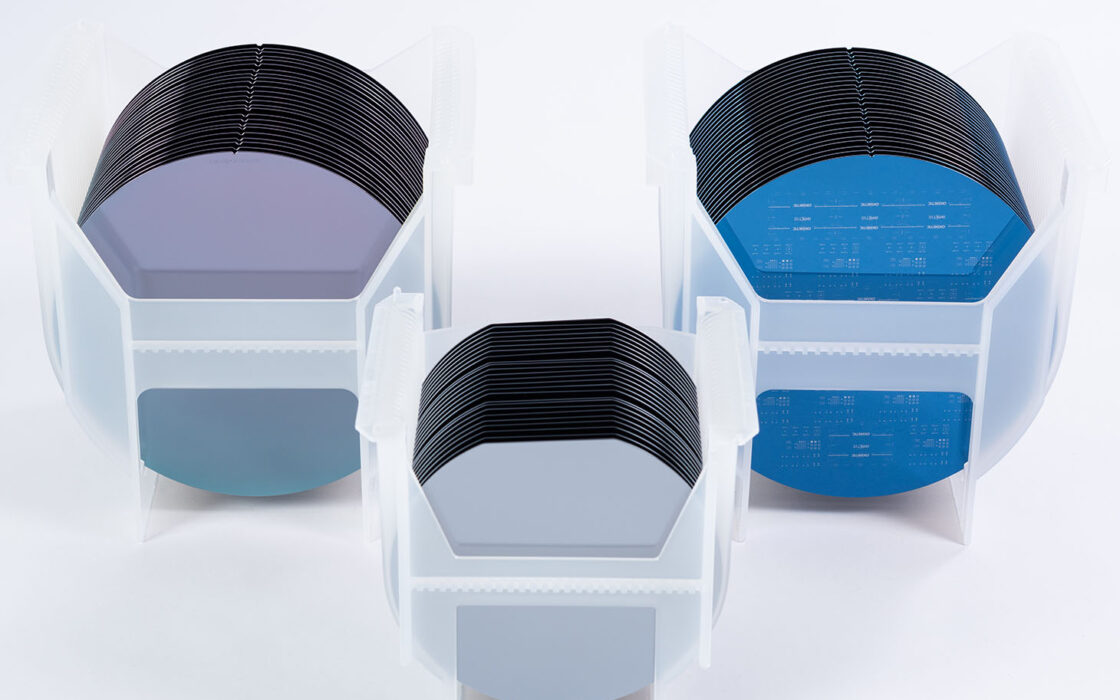
Terrace Free SOI wafers
Okmetic Terrace Free SOI wafers provide more active area and ease of processing for the SOI wafer customers. Terrace Free SOI capability is available for 200 mm Bonded Silicon-On-Insulator BSOI, E-SOI®, Power Management SOI and High Resistivity SOI wafers, which provide an optimal platform for the manufacture of MEMS, RF and power devices.
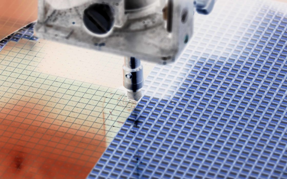
Okmetic Terrace Free SOI capability is available for the 200 mm Bonded Silicon-On-Insulator BSOI, E-SOI®, Power Management SOI and High Resistivity SOI wafers. The Terrace Free SOI wafers are manufactured with the optimized version of the established SOI process in which two wafers are bonded together and an insulating oxide layer is left between them. Typically the semiconductor devices or sensing elements are built on the top device layer whilst handle wafer is supporting the structure.
Maximized usable area and compatibility with subsequent processing
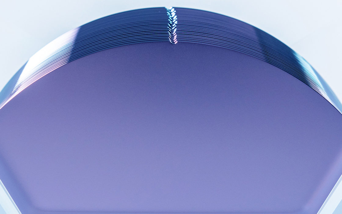
The Terrace Free SOI wafers provide device manufacturers with maximized usable area and enable more chips per wafer to be produced. The standard SOI terrace (non-SOI area) is ≤2 mm so the Terrace Free SOI wafers provide a prominent, ca. 4%, increase in the active area. Also, the Fixed Quality Area (FQA) increases by ca. 3% as a result of edge exclusion area decrease from 4.5 mm to 3.0 mm.
Terrace Free SOI wafers provide a prominent increase in the active area and fixed quality area
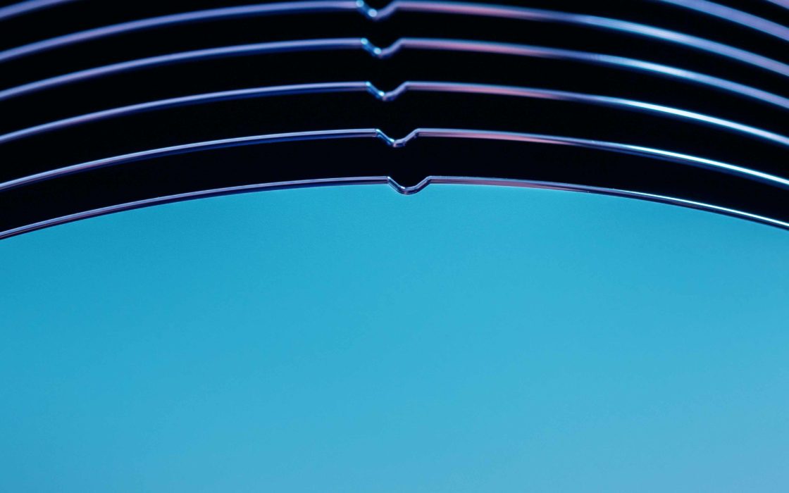
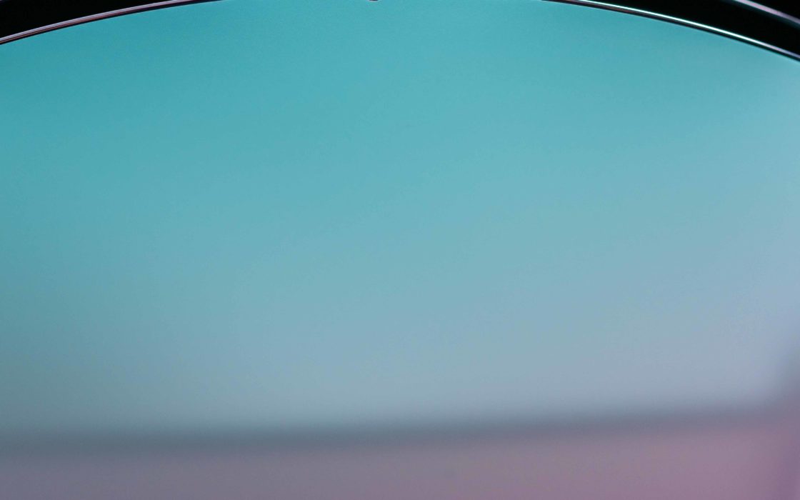
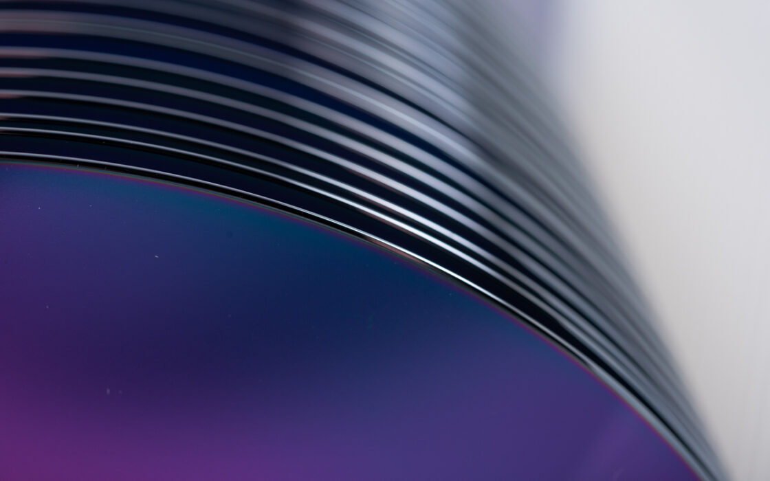
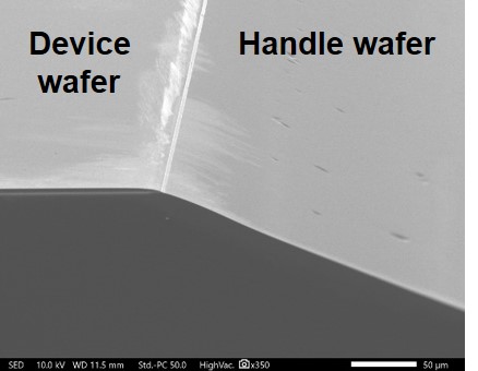
The Terrace Free SOI wafers’ edge is beveled into an optimized shape to support device processing. A precisely controlled front bevel extends to the SOI layer–BOX interface, minimizing thin silicon overhang that may arise under certain process conditions. This can help improve process robustness and consistency during critical manufacturing steps such as bonded wafer stack thinning, epitaxial growth, lithography, dicing and wafer handling.
Typical Terrace Free SOI specifications
| Growth method | Cz, MCz, A-MCz® |
| Diameter | 200 mm |
| Crystal orientation | <100>, <111>, <110> |
| N type dopants | Antimony, Phosphorus |
| P type dopants | Boron |
| Resistivity1 | <0.001 to >7,000 Ohm-cm |
| Device layer thickness2 | BSOI: From 1 µm to 150 µm, E-SOI®: From 1 μm to >40 μm, Tolerance ±0.5 µm (standard BSOI), ±0.3 µm (0.3 SOI), ±0.1 µm (200 mm E-SOI®, Power Management SOI) |
| Buried oxide layer thickness3 | From 0.1 μm to 5 μm |
| Handle wafer thickness with polished back surface4 | Exactly 500 μm, 650 μm and 725 μm thicknesses |
| Handle wafer thickness with etched back surface5 | 500-900 µm |
| Backside finishing | With or without oxide |
| Terrace area | Terrace Free |
2The thicker the device layer the longer the bevel. Some device and handle layer thickness combinations may not be feasible.
3Type: thermal oxide. Typically 0.5 μm to 2 μm. >5 μm BOX possible with certain limitations.
4Other thicknesses through feasibility study.
5Some device and handle layer thickness combinations may not be feasible.
Fully CMOS compatible wafer surface quality and cleanliness requirements
See all our 150-200 mm silicon wafers