Power Management SOI wafers
Okmetic Power Management SOI wafers are Bonded Silicon On Insulator wafers combining down to <0.001 Ohm-cm resistivity and tightly managed resistivity variation with optimized oxygen concentration and low defect density. They provide a perfect platform for power device gate drivers, Battery and Power Management ICs, Intelligent Power Modules, and other Smart Power devices using advanced BCD or BiCMOS processes.
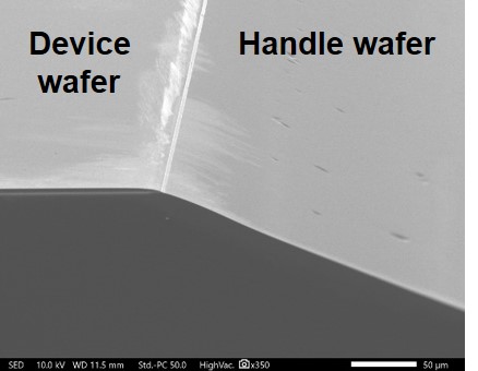
Okmetic has been supplying SOI wafers for power management devices in high volumes ever since 2015. Power Management SOI wafers are cutting edge power substrates enabling high level of integration, reduced power losses and increased yield. The wafers are manufactured by bonding two silicon wafers together and leaving an insulating buried oxide layer between them. The bonding technology enables thicker device layer for high power density needs of miniaturized chips. Moreover, our Power Management SOI wafers feature a fully customizable buried oxide layer thickness, providing improved isolation capabilities. This ensures superior high-voltage performance for power management devices.
Power Management SOI wafers enable higher current densities and improved isolation
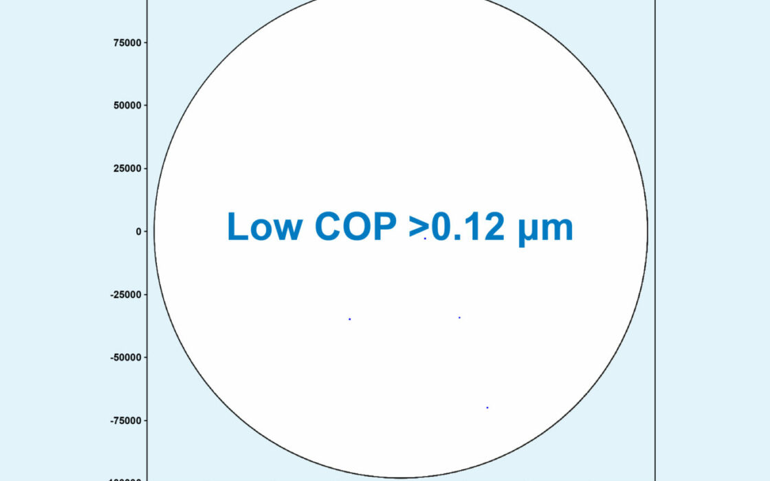
Our signature Advanced Magnetic Czochralski, A-MCz®, crystal growth method is one of the factors adding value to Power Management SOI wafers. The process enables SOI wafers with down to <0.001 Ohm-cm resistivity, tight resistivity control, low and controlled Oi levels and low amount of defects. All these factors are highly beneficial for power management devices. Read more about our Low COP SOI wafers.
In addition to Power Management SOI wafers, Okmetic also supplies SOI wafers for GaN-on-Si applications. Read more about using SOI wafers as Power GaN Substrate wafers.
Fully customizable SOI wafer solutions meeting Power Management device requirements
Power Management SOI wafers are a good match for various devices e.g. power device gate drivers (IGBT, Power MOSFET, SiC MOSFET, GaN HEMT), Battery and Power Management ICs, Intelligent Power Modules (IPMs), and other Smart Power applications using advanced BCD or BiCMOS processes, such as Power ASICs.
Power Management SOI wafers are a good match e.g. for power device gate drivers, Battery and Power Management ICs, Intelligent Power Modules and other Smart Power applications using advanced BCD or BiCMOS processes
Okmetic Power Management SOI properties are fully customizable. The device layer thickness of Power Management SOI is freely adjustable between 1.0 µm and >200 µm and the thickness tolerance is as low as ±0.1 µm (200 mm wafer) or ±0.2 µm (150 mm wafer). The thicker device layer’s benefit is that it enables higher operating current densities. The buried oxide layer thickness is also freely adjustable between 0.5 µm and 5 µm. Power Management SOI wafers are also available as Terrace Free SOI wafers providing maximized usable area.
As with other Okmetic Silicon On Insulator wafers, the Power Management SOI wafer can be customized to match your exact device and process needs. Our sales and technical support are happy to help in customization and selection of wafer parameters to find an optimal solution for your needs.
Power Management SOI wafers vs. bulk silicon wafers
SOI wafers offer extremely cost-effective solution over bulk silicon wafers. This is because SOI wafers’ layered structure allow reduced die sizes and more chips per wafer in addition to providing more design freedom. SOI wafers that are optimized for power management device also enable higher voltages and improved isolation as well as design for high common-mode transient immunity (CMTI) which is required to drive SiC and GaN HEMT power devices.
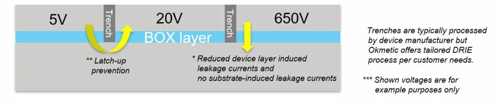
One of the Power Management SOI wafers’ key benefits compared to bulk silicon wafers is that the buried oxide layer and trench isolation enable monolithic integration of low, medium and high voltage blocks on the same chip while reducing the chip size. Power Management SOI wafers also reduce device layer induced leakage currents and generate no substrate-induced leakage currents. In addition, latch-up prevention and improved ESD/EMI protection compared to bulk silicon wafers are among the key benefits. Power Management SOI offers superior high-temperature robustness, making it an ideal choice for System-in-Package (SiP) designs. This feature allows the reduction of distance between the driver and power transistor, a critical factor, particularly for sensitive E-mode GaN HEMTs.
Power Management SOI wafer has multiple benefits:
- Effortless and more compact integration of devices operating at different voltages (low and high voltages) on a same chip
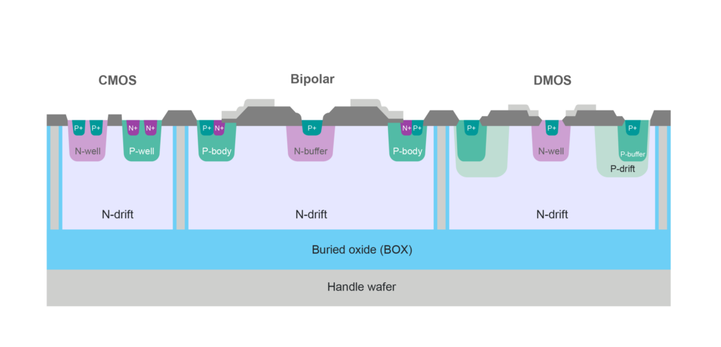
- Power transistors such as LIGBTs and LDMOSFETs can be integrated on the same chip with gate driver
- Reduced device size and improved reliability
- Reduced leakage currents minimizing power losses
- No parasitic latch-up phenomena among isolated transistors
- High temperature resilience facilitating design of high performance ICs operating in harsh environments
- Enables design for high common-mode transient immunity (CMTI)
- Effortless design and prototyping
Power Management SOI for automotive SOI-BCD
SOI-BCD-based Power ASICs are increasingly prevalent in both traditional and electric vehicles. Okmetic Power Management SOI, with its thicker device layer, can fulfill the automotive industry’s stringent demands for a wide safe operating area, exceptional thermal characteristics, and robust electrical characteristics against process variation. Additionally, SOI-BCD platforms utilizing thicker device layers offer enhanced flexibility without compromising on voltage ranges or transistor variety. Okmetic can ensure compliance with breakdown voltage requirements by mitigating the challenging back gate effect through increased device layer thickness.
Power Management SOI wafer specifications
| Growth method | Cz, MCz, A-MCz® |
| Diameter | 200 mm, 150 mm |
| Crystal orientation | <100>, <111> |
| N type dopants | Phosphorus, Red Phosphorus, Antimony, Arsenic |
| P type dopants | Boron |
| Resistivity 1 | <0.001 to >1,500 Ohm-cm |
| Resistivity tolerance | Determined per price target and resistivity range |
| Oxygen concentration (Oi)2 | <4 to 13 ppma |
| Device layer thickness3 | 1 μm to >200 μm (±0.1 µm) |
| Buried oxide layer thickness4 | 0.3 μm to >5 μm |
| Handle wafer thickness5 | 300 μm to 950 μm (±3-5 µm) |
| Back surface | Polished, etched, oxide or without oxide |
| COP amount6 | Standard or Low COP (depends on wafer size and resistivity) Zero COP SOI available with annealing process |
| Terrace area | Standard or Terrace Free (Available for 200 mm) |
2ASTM F121-831/SEMI MF1188-1107
3Other thicknesses possible with certain limitations. 150mm tolerance ±0.2 µm
4Type: thermal oxide. Typically 0.5 μm to 2 μm, >5 μm BOX possible with certain limitations
5 200 mm: typically 500-725 μm, 150 mm: typically 380-675 μm, ±3 µm tolerance for demanding devices
6 Available in 200 mm with certain limitations.
Fully CMOS compatible wafer surface quality and cleanliness requirements
See all 150-200 mm silicon wafers