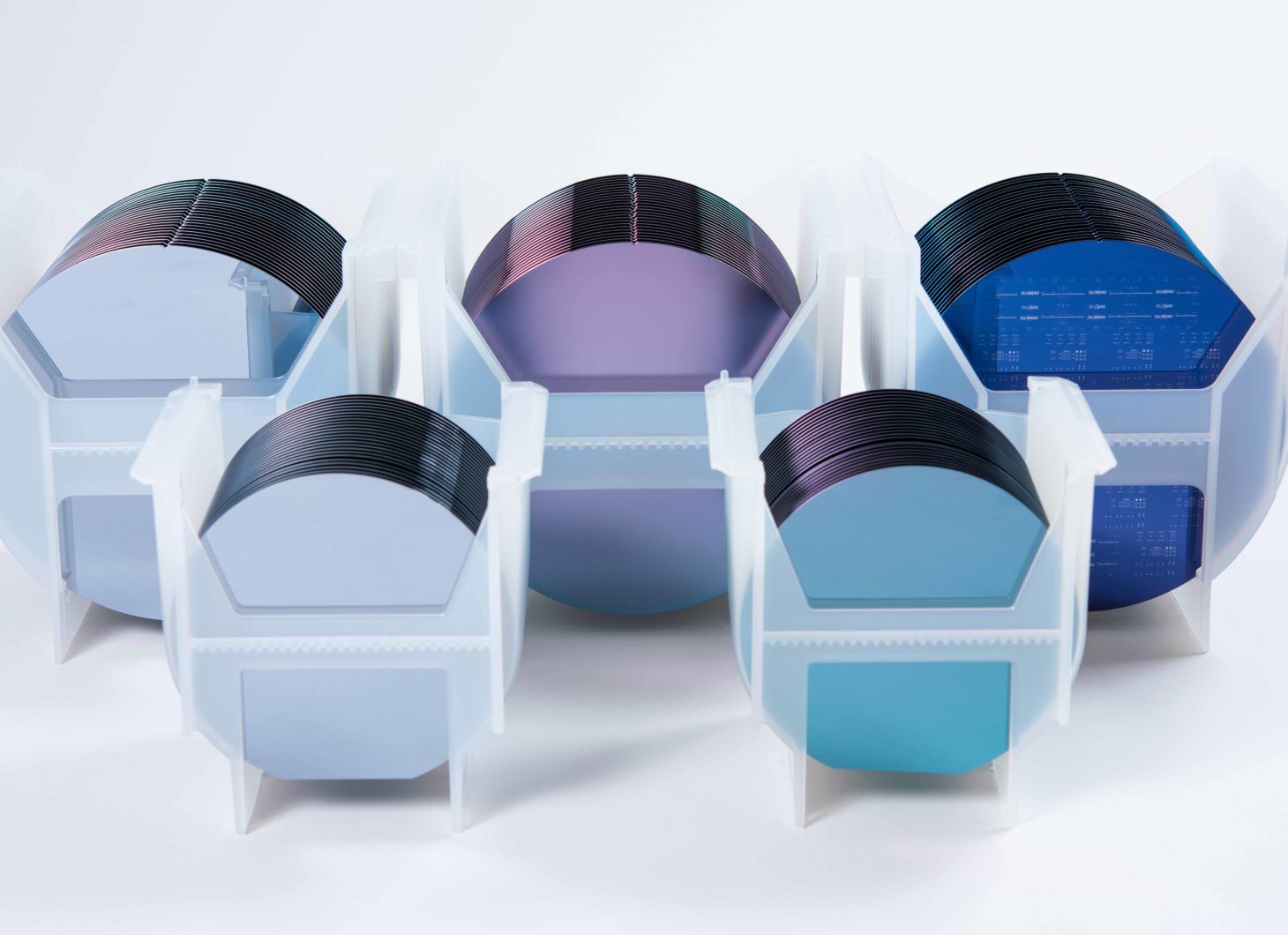
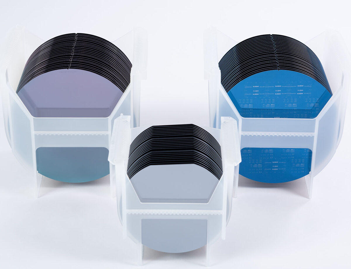
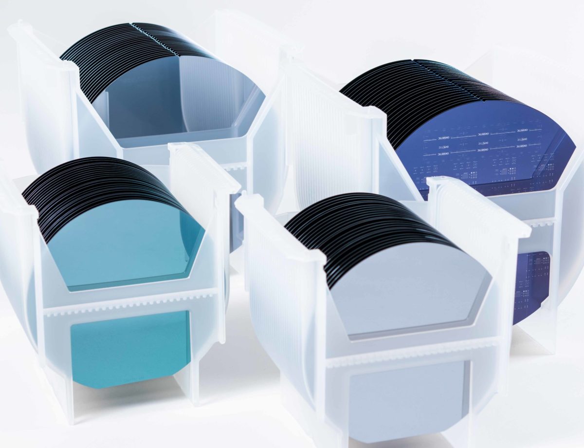
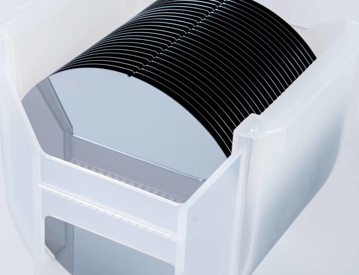
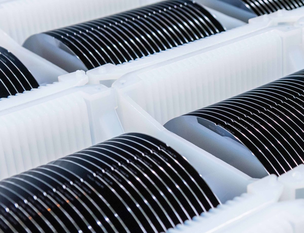
Silicon wafers 150-200 mm
Okmetic is the leading supplier of advanced, high value-added silicon wafers for the manufacture of MEMS and sensors, RF filters and devices as well as power devices. Our customized silicon wafer solutions enable high-performance devices with lower Total Cost of Ownership.
Advanced silicon wafers − Customized for your device and process needs
Okmetic is a true pioneer in silicon wafer business as it has manufactured high-performance 150-200 mm silicon wafers since 1985. What makes Okmetic’s silicon wafers unique is that each batch is tailored to the customer’s product, process and technology needs, and manufactured in volume production. This enables highly refined solutions that bring true value for the customer. Okmetic’s portfolio also extends to 300 mm wafers through strategic partner manufacturing.
Okmetic has the most extensive 150 to 200 mm silicon wafer portfolio in the market comprising of comprehensive lines of MEMS wafers, High Resistivity RFSi® wafers and Power wafers. The wafer portfolio includes Silicon On Insulator wafers, Patterned wafers, Single Side Polished, Double Side Polished wafers, EPI wafers and TSV wafers.
Advanced silicon wafers
MEMS and sensor wafer line
Okmetic MEMS and sensor wafer line provides optimal silicon and Silicon-On-Insulator wafers for the manufacture of various MEMS and sensor devices. Our MEMS and sensor device optimized silicon wafer solutions improve device performance, reduce Total Cost of Ownership and enable more refined designs.
High Resistivity RFSi® wafer line
Okmetic’s comprehensive line of high resistivity RFSi® wafers provides an optimal silicon wafer for the manufacture of RF filters and devices. Our high resistivity RFSi® wafers improve RF device performance, TCO and enable more ambitious designs.
Power wafer line
Okmetic Power wafer line provides an optimal silicon wafer for the manufacture of various power devices. Our power device optimized silicon wafer and Silicon-on-Insulator solutions improve power device performance, reduce Total Cost of Ownership and enable more refined designs.
Silicon-On-Insulator wafers
Produced with over 20 years of expertise Okmetic’s comprehensive line of bonded Silicon-On-Insulator (SOI) wafers provides an optimal platform for the manufacture of demanding MEMS, sensor, power and RF devices.
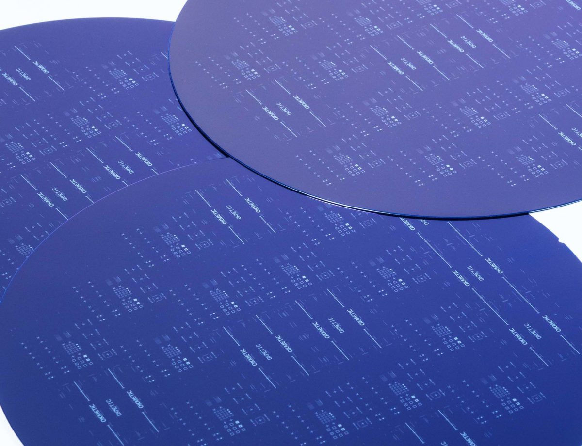
Patterned silicon wafers
Okmetic SSP, DSP and Silicon-On-Insulator wafers with built-in patterns and buried cavities (C-SOI®) enable more optimized MEMS and RF manufacturing. Fully in-house process covering crystal growth, wafering, lithography, DRIE and fusion bonded SOI guarantee supreme quality and shorter time-to-market.
Single Side Polished wafers
Okmetic Single Side Polished SSP wafers offer a perfect platform for surface MEMS, capping as well as RF and power devices. In-house crystal growing and wide selection of wafer materials enable the manufacture of customized SSP wafer solutions.
Double Side Polished wafers
Okmetic has been supplying Double Side Polished DSP wafers since 1985 and today they are used as a platform for surface MEMS, capping as well as RF and power devices. Our DSP wafers are tailored to meet each customer’s process and product specific requirements.
TSV wafers
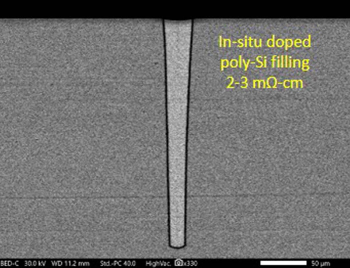
Okmetic polysilicon filled Through Silicon Vias (TSVs) enable isolated electrical connections to be made through silicon wafers, which help reduce the die size of MEMS devices and enable interlayer electrical connections and 3D MEMS integration. Our silicon wafers with TSVs are used as interposers and capping wafers in variety of sensor applications such as resonators and inertial sensors.
What is a silicon wafer?
Silicon wafers are the foundation of nearly all modern electronics. They serve as the substrate upon which integrated circuits, power devices, MEMS (microelectromechanical systems), and RF components are built. A silicon wafer is a thin, round slice of highly purified and crystallized silicon, precision-engineered to meet the demanding requirements of today’s semiconductor technologies.
At Okmetic, we specialize in manufacturing 150 mm and 200 mm silicon wafers using the Czochralski (Cz), Magnetic Czochralski (MCz), and Advanced Magnetic Czochralski (A-MCz®) crystal growth methods. To support broader semiconductor needs, we also supply 300 mm silicon wafers through strategic partner manufacturing. Our wafers are designed to meet the highest performance, quality, and uniformity standards for advanced applications across MEMS, RF and power electronics, and emerging IC markets.
The silicon wafer structure and manufacturing explained
The process of creating a high-performance silicon wafer begins with crystal growth. At Okmetic, wafers are grown using the Czochralski (Cz), Magnetic Czochralski (MCz) or Advanced Magnetic Czochralski (A-MCz®) crystal growth methods, where a single (mono) crystal silicon ingot is pulled from high-purity molten silicon. During this process, the ingot diameter is precisely controlled, determining whether the wafers will be 150 mm or 200 mm in size.
Once the ingot has been grown, it is sliced into thin, circular discs using high-precision sawing equipment. These discs, or silicon wafers, then undergo a series of critical processing steps. Each wafer is lapped, etched, and polished to create an ultra-flat, smooth surface that meets strict specifications for thickness, flatness, and cleanliness. Final cleaning removes any microscopic particles or contaminants to ensure a pristine surface for semiconductor fabrication.
The wafer’s surface serves as a platform for building layers of electronic circuits. At the fabrication stage, semiconductor device manufacturers form transistors, capacitors, sensors, and other components through a combination of photolithography, etching, ion implantation, and thin-film deposition. The material quality, flatness, and uniformity of the silicon wafer directly influence semiconductor device performance, production yield, and long-term reliability.
At Okmetic, every wafer undergoes stringent quality control checks for thickness uniformity, flatness, defectivity, and electrical properties. Our state-of-the-art facilities and process expertise enable us to maintain tight tolerances and consistent quality across production batches. While our crystal growth and manufacturing focus on 150 mm and 200 mm wafers produced using Cz, MCz, and A-MCz® methods, we also extend our portfolio to 300 mm wafers and EPI wafers through strategic partner manufacturing.
Through continuous development in crystal growth techniques and wafer processing, Okmetic ensures its wafers support innovation, reliability, and long-term performance in the global semiconductor industry.
Types of silicon wafers
Silicon wafers come in various types to meet different application needs:
Monocrystalline wafers: Produced from a single silicon crystal, offering superior electrical properties and widely used in semiconductor devices.
Polished wafers: Finished with a mirror-like surface for device fabrication. Available as single side polished (SSP) or double side polished (DSP)
Doped wafers: Silicon wafers can be doped with impurities (such as boron or phosphorus) to alter electrical conductivity, allowing the creation of p-type or n-type substrates.
Specialty wafers: These include high-resistivity, low-defect, engineered or patterned wafers for specific power, RF, or MEMS applications.
Bonded SOI (Silicon-On-Insulator) wafers: Created by bonding a thin silicon layer onto an insulating oxide layer above a silicon base wafer, SOI wafers offer superior electrical isolation, reduced parasitic capacitance, and improved device performance, particularly for MEMS, Power and RF applications.
Cavity SOI (Cavity Silicon-On-Insulator) wafers: bonded SOI wafer that has built-in sealed cavities on the handle wafer or on the buried oxide.
Silicon EPI wafers: Silicon EPI wafers are silicon substrates with a thin, high-quality epitaxial layer engineered for precise electrical performance.
At Okmetic, we provide highly customized wafers tailored to customer requirements in terms of doping, resistivity, thickness, and crystal orientation, including advanced bonded SOI wafers engineered for precision applications.
Applications of silicon wafers
Silicon wafers are the essential building blocks for a wide range of technologies, including:
MEMS and sensor devices: Critical sensing components used in automotive, medical, and consumer electronics.
Power devices: Crucial for efficient energy management in electric vehicles, renewable energy systems, and industrial equipment.
RF devices: Critical for wireless communication systems, including 4G, 5G and advanced connectivity.
Memory ICs: Supporting data storage solutions across consumer electronics, automotive, and data center applications.
Logic ICs: Enabling processing and control functions in computing, connectivity, and embedded systems.
Mixed-signal ICs: Integrating analog and digital functionality for sensing, connectivity, and control applications.
Enabling advanced applications across industries
Products manufactured by our customers using Okmetic’s high-performance silicon wafers are used across a wide range of end markets, including smartphones and portable devices, automotive electronics, industrial and healthcare systems, connectivity infrastructure, IoT devices, and energy and electrification systems. By enabling performance, reliability, and precision, our wafers support innovations that shape modern life.
What applications do 300 mm wafers support?
While 150 mm and 200 mm silicon wafers are widely used in power, MEMS, and RF applications, the semiconductor industry also employs larger 300 mm wafers that are mainly used for high-volume digital and logic integrated circuit manufacturing.
300 mm wafers are favored in semiconductor fabs producing microprocessors, memory chips, and other high-density devices due to their ability to improve economies of scale and manufacturing efficiency.
The requirements for 300 mm wafers differ significantly from those for power, MEMS, and RF devices in terms of material properties and process optimization. Okmetic’s core manufacturing expertise focuses on 150 mm and 200 mm wafers, where customization, crystal quality, and dimensional precision are critical for device performance and yield. To support broader semiconductor needs, Okmetic also supplies 300 mm wafers through strategic partner manufacturing.
Silicon wafer market growth prospects
The semiconductor industry continuously evolves, driven by increasing demands for higher performance, energy efficiency, and device integration. Silicon wafer technology remains central to this progress, and growth prospects are tied to innovations in wafer quality, size, and specialized materials.
At Okmetic, we anticipate ongoing demand for 150 mm and 200 mm wafers tailored for MEMS, RF and power electronics markets, where wafer customization and material excellence are essential. Developments in crystal growth methods and process control enable improvements in defect reduction, resistivity control, and wafer uniformity, supporting next-generation device architectures.
While the 300 mm wafer segment dominates advanced digital IC manufacturing, the mid-size wafer market remains vital for RF, power, and sensor applications, where Okmetic’s manufacturing expertise and customization capabilities deliver critical value to customers worldwide. Our portfolio also extends to 300 mm wafers through strategic partner manufacturing.
By continuously investing in advanced crystal growth technologies and quality control, Okmetic is well positioned to support the growing complexity and performance needs of semiconductor devices built on silicon wafers.