E-SOI® wafers – Enhanced SOI
Okmetic E-SOI® is an enhanced, highly uniform Silicon On Insulator wafer with tight ±0.1 µm thickness tolerance. The combination of thicker device layer and significantly lower device layer thickness variation makes E-SOI® an ideal platform for demanding MEMS and sensor devices as it enables device designs out of reach with traditional techniques in addition to improved device performance and precision.
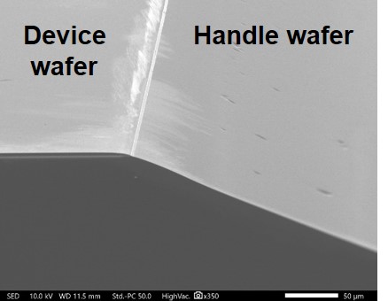
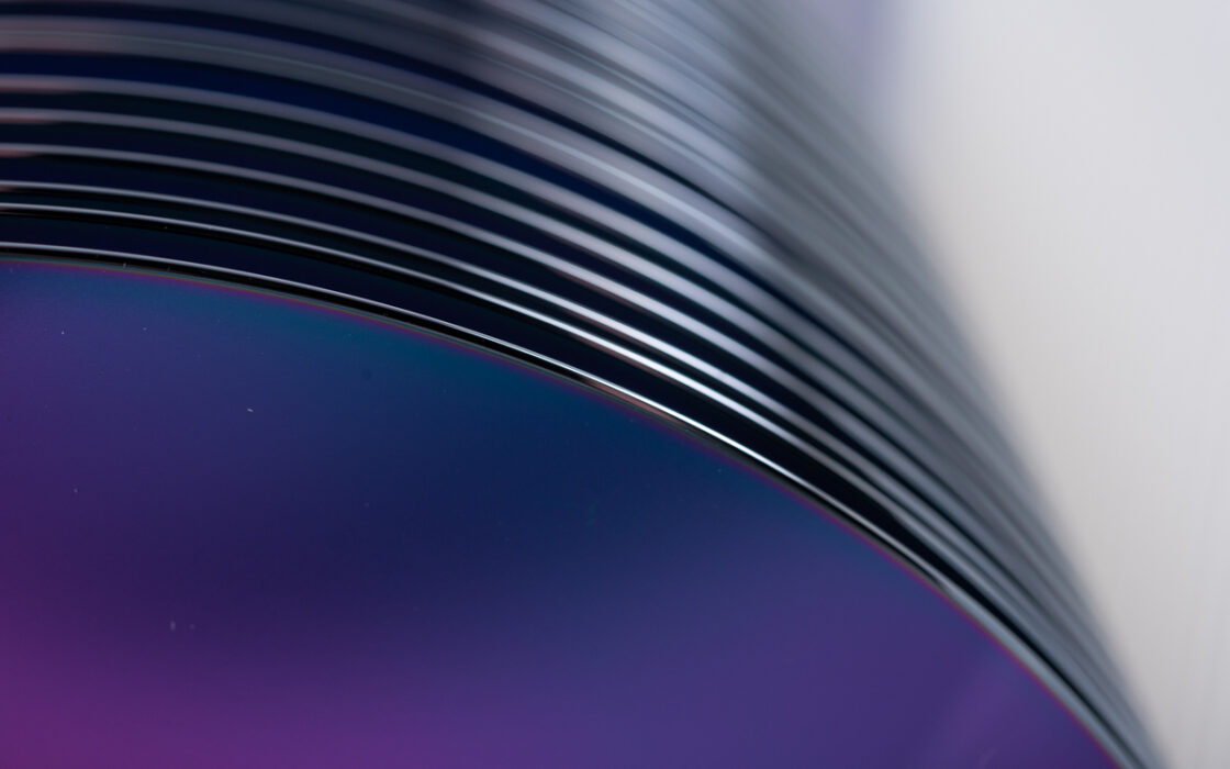
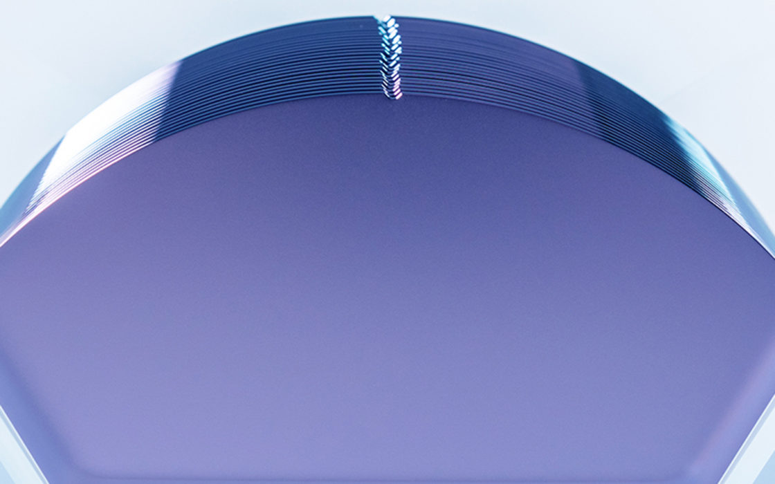
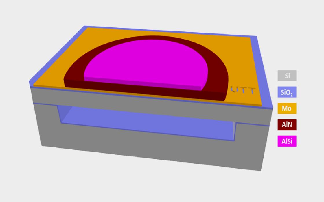
Okmetic E-SOI® is an enhanced bonded Silicon On Insulator wafer, which has buried oxide (BOX) layer between a bottom handle wafer and a top silicon wafer that is thinned with extreme precision to achieve best-in-class device layer thickness uniformity. Enhanced SOI (E-SOI®) wafer’s device layer can be made thicker and more uniform than with competing SOI technologies.
E-SOI® wafer’s best-in-class device layer thickness uniformity enables the most demanding device designs
Typically MEMS sensors are built on the device layer whilst the buried oxide (BOX) is an excellent electric insulating layer and an effective etch stop. The BOX layer can also act as a sacrificial layer for complex components and released structures. The handle wafer supports the structure, but can also be utilized in sealing the structure or as part of the sensing element.
E-SOI® wafers’ additional manufacturing step enables exceptionally low device layer thickness variation that helps maintain precise dimensional control across the wafer, supporting improved device performance and more consistent device characteristics.
Enhanced SOI wafer for demanding device needs
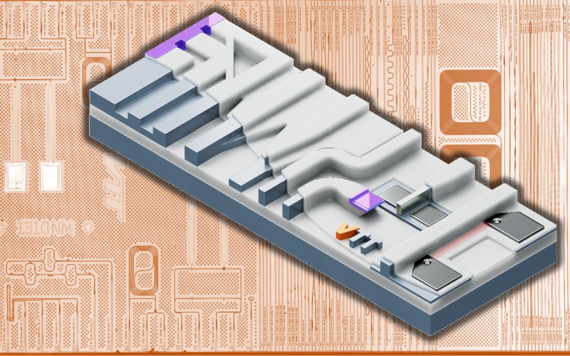
Due to its thicker and highly uniform device layer, Okmetic E-SOI® wafer is an ideal platform for demanding applications such as high-precision silicon-based MEMS and sensors. Typical applications include photonic integrated circuits (PICs), pressure sensors, silicon microphones, silicon timing devices, MEMS resonators, PMUT (Piezoelectric Micromachined Ultrasonic Transducer) and CMUT devices, and advanced cooling devices requiring highly uniform silicon structures. Okmetic also suppliers Power Management SOI wafers that combines E-SOI® benefits to other power management optimized wafer characteristics.
Okmetic E-SOI® has unprecedented properties. The device layer thickness of Enhanced SOI is freely adjustable between 1.0 µm and >40 µm and the thickness tolerance is as low as ±0.1 µm (200 mm wafer) or ±0.2 µm (150 mm wafer). Also the buried oxide layer thickness is freely adjustable between 0.5 µm and >5 µm.
E-SOI® wafer is an ideal platform e.g. for silicon photonics and timing devices, and high-precision MEMS sensors
The exceptional device layer thickness uniformity of E-SOI® wafers enables tighter control of critical device dimensions. Reduced device layer thickness variation helps minimize variation in mechanical, electrical and optical device characteristics, supporting improved repeatability and manufacturing consistency across the wafer. This can improve device precision, performance and reliability while providing greater design flexibility. For many MEMS and photonics applications, it also supports smaller device dimensions.
E-SOI® wafers are used especially in silicon photonics, a rapidly growing field including applications such as photonic integrated circuits (PICs), optical transceivers, optical sensors and LiDAR devices. The highly uniform device layer thickness helps maintain tight waveguide dimensional control across the wafer, supporting consistent optical characteristics and manufacturing repeatability. Read more about E-SOI® wafers providing excellent waveguide for silicon photonics.
For resonant devices such as timing devices, MEMS resonators and gyroscopes, improved thickness control can help reduce resonance frequency variation and improve device consistency. In pressure sensing applications, precise layer thickness helps maintain membrane uniformity, supporting improved device precision and enabling smaller device dimensions. Similar benefits can support PMUT devices and advanced cooling devices that require highly uniform silicon structures and precise dimensional control.
As with other Okmetic Silicon On Insulator wafers, the E-SOI® wafer can be customized to match your exact device and process needs. E-SOI® wafers can be customized at device layer, buried oxide (BOX) and handle wafer level, enabling optimization for specific photonics, MEMS, timing device, and PMUT requirements.
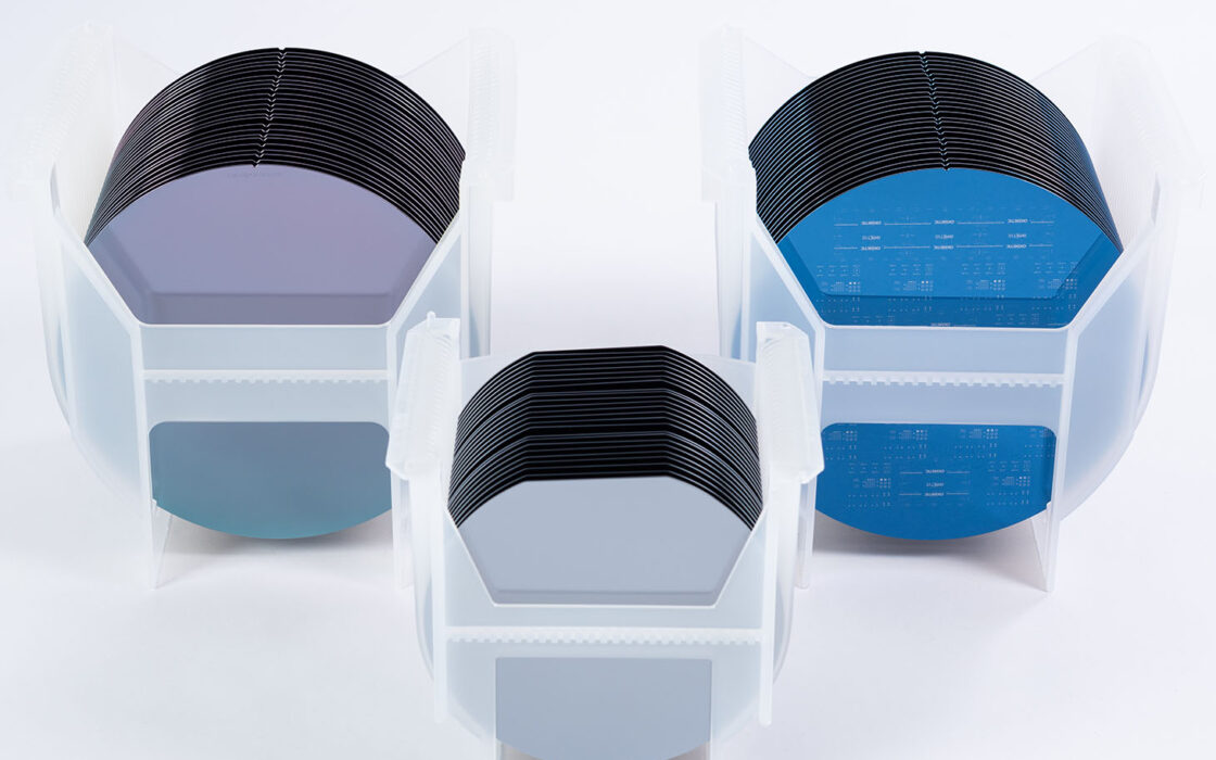
Okmetic has the widest selection of silicon wafers in the market, and our sales and technical support are happy to help in customization and selection of wafer parameters to find an optimal solution for your needs. E-SOI® wafers are also available as Terrace Free SOI wafers.
Typical SOI specifications
| Growth method | Cz, MCz, A-MCz® |
| Diameter | 200 mm, 150 mm |
| Crystal orientation | <100>, <110>,<111> |
| N type dopants | Antimony, Phosphorus |
| P type dopants | Boron |
| Resistivity1 | From <0.001 to >7,000 Ohm-cm |
| Device layer thickness2* | BSOI: From 1 μm to >200 μm, E-SOI®: From 1 μm to >40 μm, Tolerance ±0.5 μm (standard BSOI), ±0.3 μm (0.3 SOI), ±0.1 μm (E-SOI®, Power Management SOI), ±0.5 μm or lower (C-SOI®) |
| Buried oxide layer thickness3 | From 0.3 μm to >5 μm |
| Handle wafer thickness4 | 200 mm: 300 μm to 950 μm 150 mm: 300 μm to 950 μm |
| Back surface | Polished or etched |
| Terrace area | Standard or Terrace Free (Available for 200 mm BSOI, E-SOI®, Power Management SOI, High Resistivity SOI) |
2Other thicknesses possible with certain limitations. 150 mm E-SOI® tolerance ±0.2 µm
3Type: thermal oxide. Typically 0.5 μm to 2 μm. >5 μm BOX possible with certain limitations.
4200 mm: typically 500-725 μm, 150 mm: typically 380-675 μm. ±3 µm tolerance for demanding devices
*Possibility also for two device and buried oxide layers with different thicknesses.
Fully CMOS compatible wafer surface quality and cleanliness requirements
Significantly lower device layer thickness variation enabling true innovation
The core benefit of E-SOI® wafer compared to standard BSOI wafer is superior device layer thickness uniformity. The exceptionally low device layer thickness variation enables tighter thickness control across the wafer and supports advanced device designs requiring high dimensional accuracy. E-SOI® thus enables more advanced device designs than can be achieved with traditional Bonded SOI technologies let alone with bulk silicon micromachining.
Superior device layer thickness uniformity enables tighter control of critical device structures, helping reduce process variation and improve repeatability across the wafer. This is particularly important in silicon photonics, timing devices, PMUT and CMUT devices, cooling devices and precision MEMS sensors where dimensional accuracy directly impacts device performance.
Device layer thickness capability of E-SOI® wafers
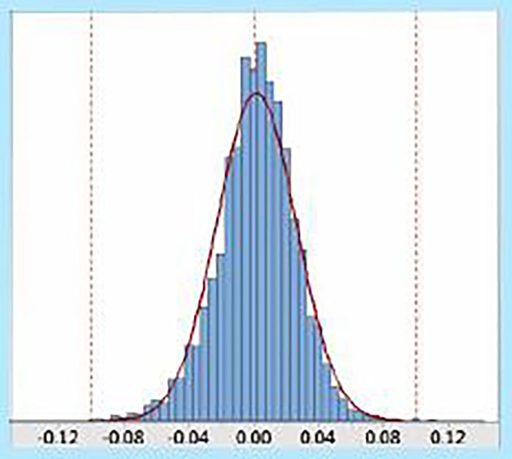
Deviation from target thickness (µm)
E-SOI® wafer is an advanced solution with multiple benefits:
- More freedom to device design than with competing technologies
- Improved device performance and precision
- Reduced device size and cost
- Improved device yield
See all our 150-200 mm silicon wafers