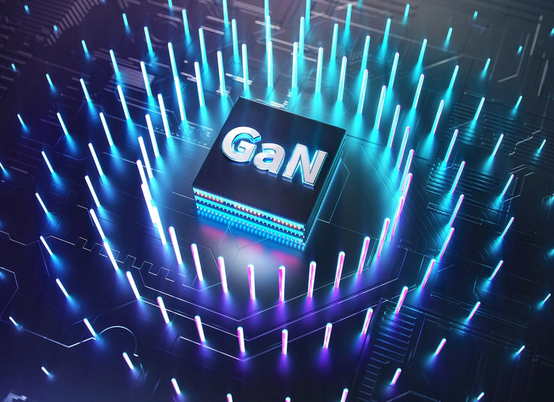
Power GaN Substrate wafers (Si and SOI)
Okmetic Power GaN Substrate wafers comprise standard to extra thick, <111> oriented SSP, DSP and Bonded SOI wafers that offer advanced stress management for GaN growth. The Power GaN Substrate wafers provide a highly functional and cost-effective challenger for GaN–on-SiC substrates and are suitable for power GaN devices such as GaN HEMT devices.
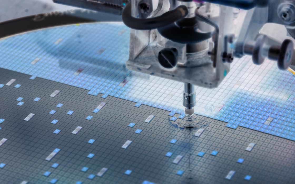
Okmetic has been in the forefront developing substrate wafers to match the demanding power GaN epitaxial process needs. Various wafer design characteristics determine how the silicon substrate wafers behave in the GaN epitaxial process. Okmetic’s vast expertise has enabled to design silicon substrate wafers that endure the demanding GaN epitaxial process conditions and provide reduced wafer bow and warpage.
Silicon substrate wafers that are designed to endure the demanding GaN epitaxial process conditions and provide reduced wafer bow and warpage
In addition to the SSP, DSP and SOI Substrate wafers optimized for Power GaN application needs, Okmetic also supplies high resistivity RF GaN Substrate wafers. Learn more about Okmetic GaN Substrate benefits from our White paper: Enabling next-gen power and RF GaN devices with optimized silicon and SOI substrates.
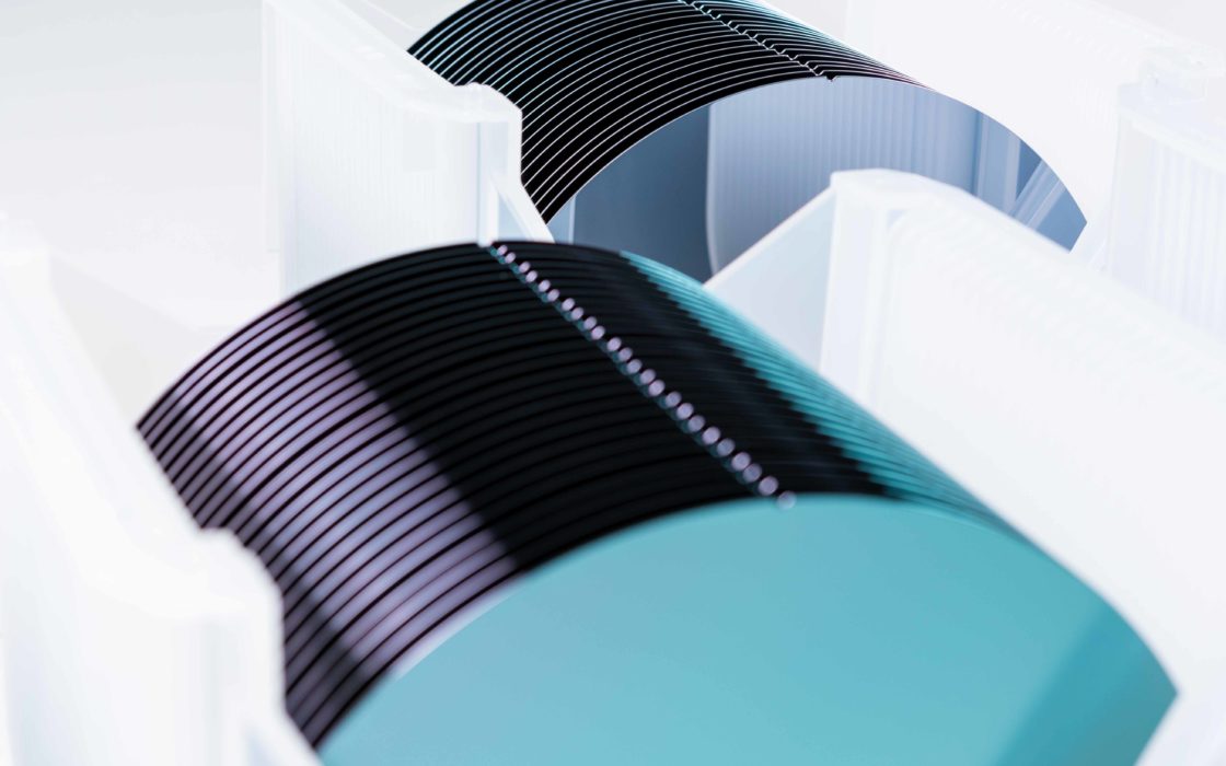
Silicon substrate wafers optimized to endure GaN processes’ extreme stresses
Okmetic Power GaN Substrate wafers (SSP and DSP) are designed to endure the extreme stresses of the GaN epitaxial process and provide reduced wafer bow and warpage. Our signature Advanced Magnetic Czochralski, A-MCz®, crystal growth method is one of the factors adding value to Power GaN Substrate wafers. The process enables Power GaN Substrate wafers with ultra high dopant concentration and controlled Oi guaranteeing the best lattice integrity. Additional stress management is gained through tight and optimized orientation control.
Durable wafers with maximum performance
- Designed to endure the extreme stresses of the GaN epitaxial process and to reduce power losses
- Low resistivity with high doping and optimized Oi for increased lattice integrity and durability
- Customized solutions for different needs
Fully customizable for your process needs
Power GaN Substrate wafers (SSP and DSP) for GaN-on-Si applications can be customized for even beyond 650 V lateral GaN HEMT devices and high power LEDs, providing a highly functional and cost-effective challenger for GaN-on-SiC substrates.
Power GaN Substrate wafers can be customized for even beyond 650 V lateral GaN HEMT devices and high power LEDs
Okmetic Power GaN Substrate wafers can be fully customized for your device and process needs. The substrate wafers are available both in on and off orientation <111> with tight orientation control. The wafer thicknesses range from standard to extra thick 1,150 µm wafer thickness providing reduced wafer bow and warpage as well as increased wafer durability. Back surface options include Poly and LTO, which provide further stress management.
Silicon vs. Silicon carbide
Silicon’s popularity as GaN substrate is rising as it offers a cost-effective platform for higher voltage power devices challenging existing GaN-on-SiC platforms. Silicon substrate wafers’ main benefit over silicon carbide substrate wafers in addition to cost-efficiency is that they are readily available in 200 mm diameter.
SOI Substrate wafers are an emerging solution for monolithic integration of GaN devices
SOI wafers have become a viable solution for the monolithic integration of GaN devices. They are a good match for low-stress GaN HEMT, integrated direct drive/cascode GaN HEMT and monolithic all GaN integration.
In a collaboration project with IMEC, IMEC successfully grew a 4.4 µm GaN-epi-stack on Okmetic wafers, with the GaN-optimized SOI wafers showing superior GaN layer uniformity, reduced wafer bowing, and enhanced electrical performance in post-growth studies. Read about the collaboration results from here. Earlier, GaN layers grown on Bonded SOI wafers exhibited lower stress and higher crystalline quality according to x-ray diffraction than the layers grown on standard silicon substrates. Read more about the results from here.
The combination of BOX layer and trench isolation enables monolithic integration reducing die size as well as gate driver integration near the GaN device. The latter increases power efficiency, reduces ringing and increases voltage budget for E-mode GaN driver design as the gate voltage noise and over/undershoot is reduced.
In a collaboration project with IMEC, a 4.4 µm GaN-epi-stack was successfully grown on Okmetic’s GaN-optimized SOI wafers, demonstrating superior GaN layer uniformity, reduced wafer bowing, and enhanced electrical performance.
Okmetic GaN SOI Substrates are fully customizable. They combine down to <0.001 Ohm-cm resistivity with controlled Oi enabling excellent lattice integrity. On-orientation <111> with tight orientation control increases durability, but good results can also obtained with off-oriented wafers. The device, handle and BOX layer are fully customizable. Handle wafer thickness can be adjusted up to 950 µm for reduced wafer bow and increased durability. The buried oxide layer thickness is also freely adjustable between 0.5 µm and 4 µm. GaN SOI Substrate wafers are also available as Terrace Free SOI wafers, which enable maximized usable area and optimal edge shape.
Power GaN Substrate wafer specifications for GaN-on-Si applications
| Growth method | MCz, A-MCz® |
| Diameter | 200 mm, 150 mm |
| Crystal orientation | <111>, off-oriented possible |
| N type dopants | (Phosphorus, Antimony, Arsenic) |
| P type dopants | Boron |
| Resistivity1 | <0.001 to >1,500 Ohm-cm |
| Resistivity tolerance | Determined per price target and resistivity range |
| Oxygen concentration (Oi)2 | <4 to 20 ppma |
| Radial oxygen gradient (ROG)3 | Typically below 10% |
| Carbon concentration4 | <0.5 ppma |
| SSP wafer thickness5 | 200 mm: 550 to 1,150 µm 150 mm: 400 to 1,150 µm |
| DSP wafer thickness5 | 200 mm: 380 to 1,150 µm 150 mm: 380 to >1,150 µm |
| SSP backside treatment | Etched, Polyback, LTO |
2ASTM F121-831/SEMI MF1188-1107
3SEMI MF951, low Oi: ROG >20%
4ASTM F123-91, limited by measurement technology
5Other thicknesses possible with certain limitations.
Fully CMOS compatible wafer surface quality and cleanliness requirements
Power GaN Substrate wafer specifications for GaN-on-SOI applications
| Growth method | MCz, A-MCz® |
| Diameter | 200 mm, 150 mm |
| Crystal orientation | <111>, off-oriented possible |
| N type dopants | (Phosphorus, Antimony, Arsenic) |
| P type dopants | Boron |
| Resistivity1 | <0.001 to >1,500 Ohm-cm |
| Resistivity tolerance | Determined per price target and resistivity range |
| Oxygen concentration (Oi)2 | <4 to 13 ppma |
| Device layer thickness3 | 2 μm to >200 μm (±0.1 µm) |
| Buried oxide layer thickness4 | 0.3 μm to >5 μm |
| Handle wafer thickness5 | 675 μm to 950 μm (±3-5 µm) |
| Back surface | Polished or Etched |
| Terrace area | Standard or Terrace Free (Available for 200 mm) |
2ASTM F121-831/SEMI MF1188-1107
3Other thicknesses possible with certain limitations. 150mm tolerance ±0.2 µm
4Type: thermal oxide. Typically 0.5 μm to 2 μm, >5 μm BOX possible with certain limitations.
5200 mm: typically 725 μm, 150 mm: typically 675 μm, ±3 µm tolerance for demanding devices
Fully CMOS compatible wafer surface quality and cleanliness requirements
See all 150-200 mm silicon wafers