RF filters and devices
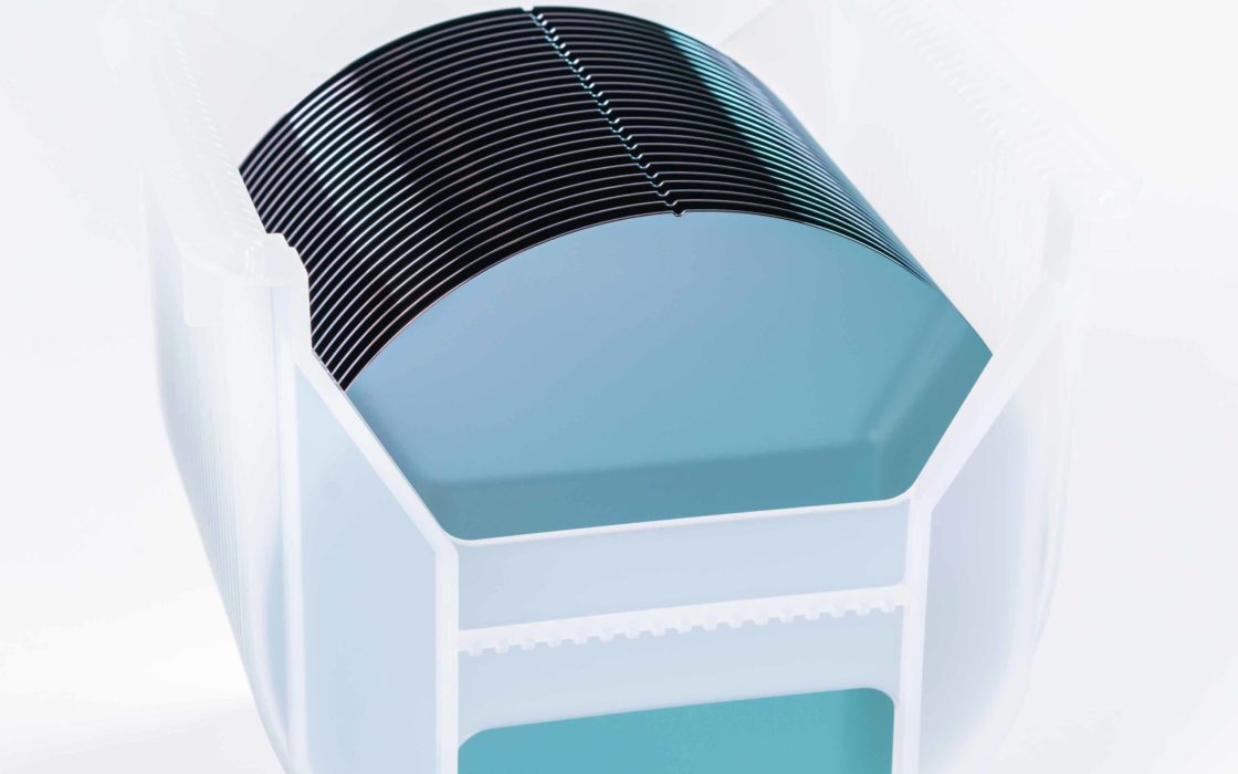
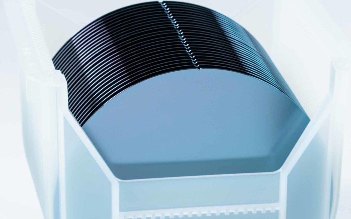
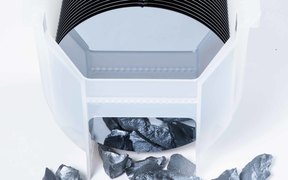
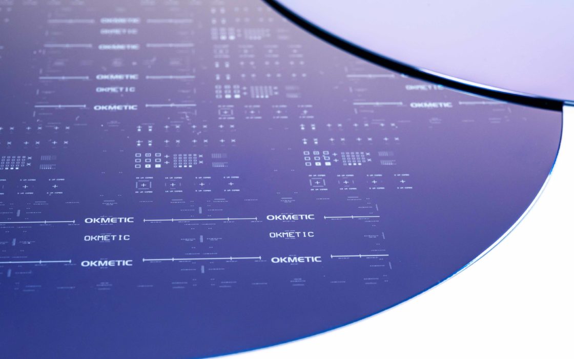
Silicon wafers have a great effect on device performance, Total Cost of Ownership and time to market. This is why device manufacturers are paying more attention to the choice of substrate and the demand for device and process optimized substrates is increasing.
Finding an optimal silicon wafer platform for one’s device and process needs isn’t always easy. To make the search easier we have compiled an indicative and non-exhaustive list of RF filters and devices and suitable wafer options below. Our sales and technical support are happy to help you find a perfect silicon solution for your device and process needs.
Learn more about our Engineered high resistivity wafer benefits from our White paper: Advancing from 4G LTE to 5G and 6G: Engineered RFSi® silicon wafers for high-performance RF devices and about our GaN substrate wafer benefits from our White paper: Enabling next-gen power and RF GaN devices with optimized silicon and SOI substrates.
BAW filters
High Resistivity wafers with stable low Oi offer perfect platform to drive the insertion losses lower. Pairing these with proprietary parasitic suppression layer enabled by Engineered High Resistivity wafers will give the highest effective resistivity, record low insertion losses, superior 2nd harmonic values as well as excellent linearity over temperature. Such wafers characteristics can also be combined with suspended C-SOI® structures to serve in the latest resonator type structures used in RF industry. Learn more about our High Resistivity Bonded SOI wafers.
TF-SAW filters
Low-loss engineered high resistivity wafers with ultra-flat properties is the key for the latest high performance Thin Film SAW filters. Symmetrical, very flat silicon surface allows economical and precise thin film manufacturing on top. Customized turnkey trap-rich layer on top of the silicon wafer helps optimize the loss and linearity characteristics of the filter. Learn more about our UF-RFSi® wafers. Other suitable wafer types are Engineered High Resistivity and Engineered Ultra High Resistivity wafers both combining highly efficient trap-rich layer and high resistivity.
IPD devices
High Resistivity wafers with stable low Oi offer perfect platform to drive the insertion losses lower. Pairing these with proprietary parasitic suppression layer enabled by Engineered High Resistivity wafers will give the highest effective resistivity, record low insertion losses, superior 2nd harmonic values as well as excellent linearity over temperature. Such wafers characteristics can also be combined with suspended C-SOI® structures to serve in the latest resonator type structures used in RF industry. Learn more about our High Resistivity Bonded SOI wafers.
Power amplifiers
RF Gan Substrate wafers with 111 orientation and optimized Oi to help fight the stresses in Customer GaN-on-Si process. The high resistivity bulk properties of these wafers keep insertion losses low. Excellent off-orientation control to enable accurate and successful GaN epi layer.
High Resistivity Bonded SOI wafer can also be used as an advanced GaN-on-Si substrate. SOI structure coupled with deep trench isolation enables monolithic integration of the power device, driver and logic to the same chip. Insulating oxide eliminates harmful back-gate effect which reduces switching noise. High operating frequency on such platform means fast switching device with smaller die size. Using Bonded SOI wafer as a platform offers an excellent way to shrink the die architecture.
Integrated RFIC
Integrated RFIC applications benefit from High Resistivity and Engineered High Resistivity wafers with controlled bulk properties yielding to very high, stable resistivity and good electric performance.
Silicon interposers
Thin High Resistivity and Engineered High Resistivity wafers with excellent flatness and high, stable resistivity to enable more economical device integration in Wafer Level Packaging. These wafers can have TSV (Through Silicon Vias) incorporated to them to further enhance the vertical packaging options.