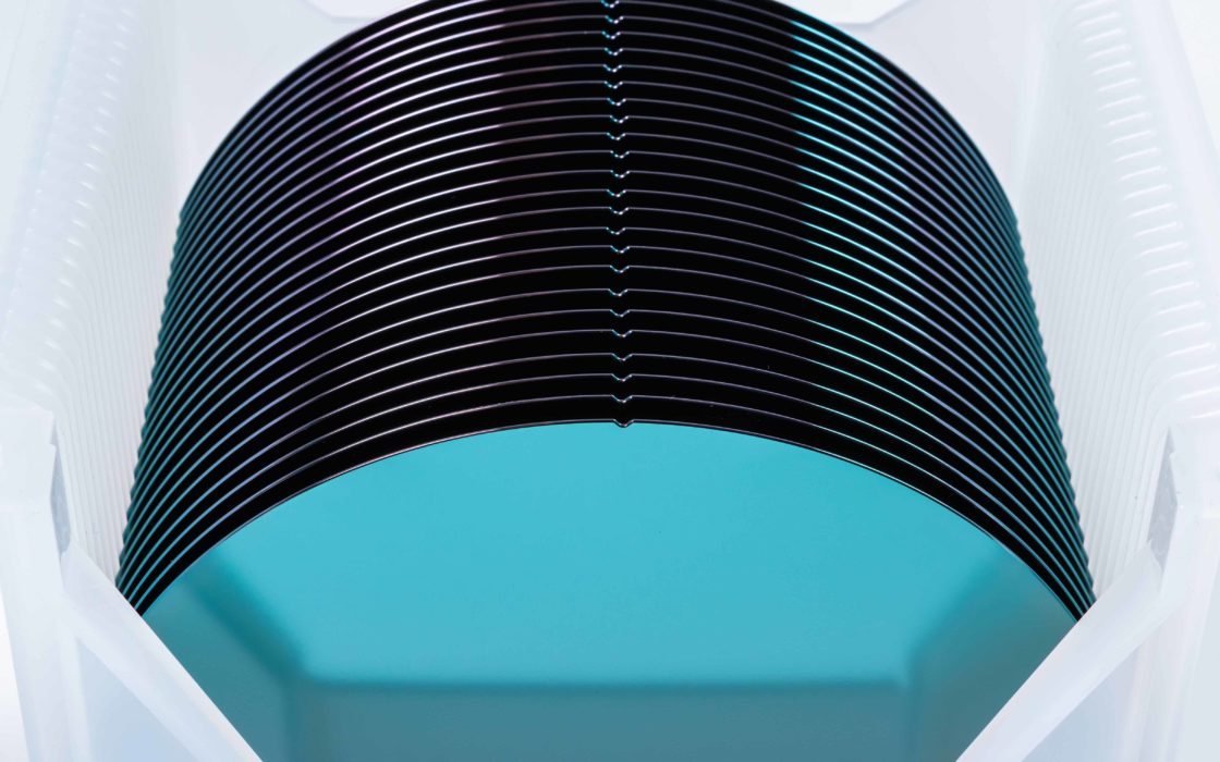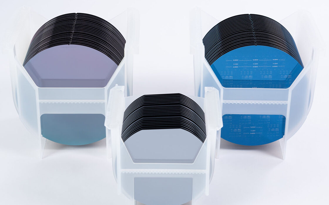
BSOI wafers – Bonded SOI
Okmetic Bonded Silicon On Insulator wafers offer advanced platform for MEMS and sensor devices. In many cases BSOI wafers are more cost-effective choice than bulk silicon wafers. BSOI wafers have many benefits as they enable more ambitious device designs, improved device performance and smaller die size and they can be fully customized to meet your device and process needs.
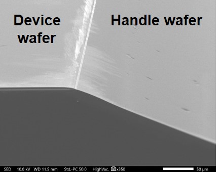
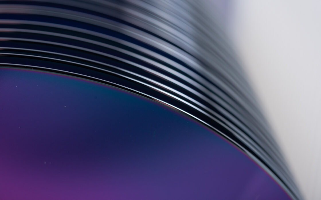
Okmetic BSOI wafers are manufactured by bonding two silicon wafers together leaving an insulating buried oxide layer between them. Typically sensing elements and possible IC devices are built on the top wafer acting as a device layer. The buried oxide layer is an excellent electric insulating layer and it also forms an effective etch-stop in device manufacturing. It can also act as a sacrificial layer when manufacturing more complex devices such as released MEMS structures. The handle wafer is supporting the structure but can also be utilized in sealing the structure or as part of the sensing element. SOI wafers’ quality and cleanliness standards are identical with bulk silicon wafers.
Bonding and thinning process enables thicker SOI device layer than competing technologies, which gives more device design freedom
Thanks to Okmetic’s bonding and thinning process, the device layer of the SOI wafer can be made much thicker than with competing SOI technologies, which gives more freedom to device design. The Bonded SOI wafer device layer can range from 1 μm to over 200 μm with standard thickness tolerance being ±0.5 µm and even ±0.1 µm with Enhanced SOI. Okmetic’s superior orientation accuracy capability can be utilized in both device layer and handle wafer, which enables smaller variation in customer’s device performance. Handle wafer thicknesses between 300 µm and 950 µm are possible and back surface can be polished or etched. Buried oxide is high quality thermally grown SiO2.
BSOI wafers are optimal for variety of devices
Okmetic BSOI wafer solutions are used e.g. for pressure sensors, microfluidic devices, MOEMS, flow sensors, actuators, cooling devices, 3-axis accelerometers, gyroscopes, silicon speakers, quantum devices and mechanical parts. SOI wafers are used more and more in the manufacture of gate drivers (IGBT/Power MOSFET), Battery and Power Management ICs etc., read more about our Power Management SOI wafers. In addition, SOI wafers usage is expanding into RF field, for the needs of which Okmetic has developed High Resistivity SOI wafers. The possibility to tailor and modify parameters helps reach the full potential of any design idea in advanced device development. BSOI wafers are now available as Terrace Free SOI wafers.
Typical SOI specifications
| Growth method | Cz, MCz, A-MCz® |
| Diameter | 200 mm, 150 mm |
| Crystal orientation | <100>, <110>,<111> |
| N type dopants | Antimony, Phosphorus |
| P type dopants | Boron |
| Resistivity1 | From <0.001 to >7,000 Ohm-cm |
| Device layer thickness2* | From 1 μm to >200 μm Tolerance ±0.5 μm (standard BSOI), ±0.3 μm (0.3 SOI), ±0.1 μm (E-SOI®, Power Management SOI), ±0.5 μm or lower (C-SOI®) |
| Buried oxide layer thickness3 | From 0.3 μm to >5 μm |
| Handle wafer thickness4 | 200 mm: 300 μm to 950 μm 150 mm: 300 μm to 950 μm |
| Back surface | Polished or etched |
| Terrace area | Standard or Terrace Free (Available for 200 mm BSOI, E-SOI®, Power Management SOI, High Resistivity SOI) |
2Other thicknesses possible with certain limitations. 150 mm E-SOI® tolerance ±0.2 µm
3Type: thermal oxide. Typically 0.5 μm to 2 μm. >5 μm BOX possible with certain limitations.
4200 mm: typically 500-725 μm, 150 mm: typically 380-675 μm. ±3 µm tolerance for demanding devices
*Possibility also for two device and buried oxide layers with different thicknesses.
Fully CMOS compatible wafer surface quality and cleanliness requirements
BSOI wafers enable more ambitious device designs cost-effectively
SOI wafers offer extremely cost-effective solution over bulk silicon micromachining. As an example, when manufacturing a pressure sensor on 400 µm thick wafer the cost per chip can be reduced by 33% with BSOI wafer compared to bulk silicon micromachining. This is because BSOI wafers allow smaller die sizes and more chips per wafer thus reducing the wafer, patterning, etching and bonding costs.
The BSOI wafer enables the design of more advanced applications thanks to its layered structure and possibility for a thicker device layer adding the design freedom. For example, expansion of smart power management integrations to include High Voltage driver circuits up to 100V or beyond are possible when using BSOI wafer as a platform.
BSOI wafer is an advanced solution with multiple benefits:
- Reduced device size and cost
- Improved device performance and precision
- Increased device reliability
- More advanced device designs
BSOI variations for specialized needs
0.3 SOI wafers
Okmetic 0.3 SOI is a bonded Silicon On Insulator wafer, which has buried oxide (BOX) layer between a bottom handle wafer and a top silicon wafer that is thinned with extra precision to achieve improved ±0.3 μm device layer thickness tolerance. This improved device uniformity is a relatively cost-effective solution enabling improved device performance and precision and additional freedom to device design. Even higher uniformity can be achieved with Okmetic E-SOI® wafers. The 0.3 SOI wafer is beneficial platform for many MEMS devices such as pressure sensors and resonators.
DSOI wafers
Okmetic DSOI is a bonded Silicon On Insulator wafer, that has two device and buried oxide layers with different thicknesses. The D-SOI wafer is beneficial platform for MEMS and photonics devices.
LSOI wafers
Okmetic LSOI is a bonded Silicon On Insulator wafer combining thick and highly doped device layer. This kind of Low Resistivity Bonded SOI wafer is beneficial in certain MEMS devices eg. silicon oscillators as no external packaging is needed unlike with quartz-based oscillators. This leads to reduced board size an absence of quality issues with external chips.
Thick SOI wafers
Okmetic Thick SOI is a bonded Silicon On Insulator wafer with very thick device layer. The bonding process enables the manufacture of very thick, over 200 μm SOI device layers that would not be possible with other competing technologies.
See all our 150-200 mm silicon wafers