High Resistivity BSOI wafers
Okmetic High Resistivity Bonded SOI wafers with suspended low-loss structures are designed for the demanding needs of devices operating in the high frequency mm wave bands.
Okmetic’s in-house process from crystal growth and wafering to patterning and SOI gives Okmetic ability to combine technologies and offer customers new types of value-added wafer solutions for the demanding needs of mm wave devices. Okmetic High Resistivity Bonded Silicon On Insulator wafers with suspended low-loss structures enable lumped element solutions combined with novel approaches such as strip line filters, which are a promising new technology. Low-loss device layer material can also be combined with turnkey cavity SOI structures (C-SOI®) to create a platform for new type of BAW resonators or IPD devices. Simplified structures for integrated sensors and communications chips are available also for strip line platforms.
Okmetic’s expertise and ability to combine technologies enables new types of value-added wafer solutions for the demanding needs of mm wave devices.
High and stable resistivity combined to uniform device layer with flexible thickness target
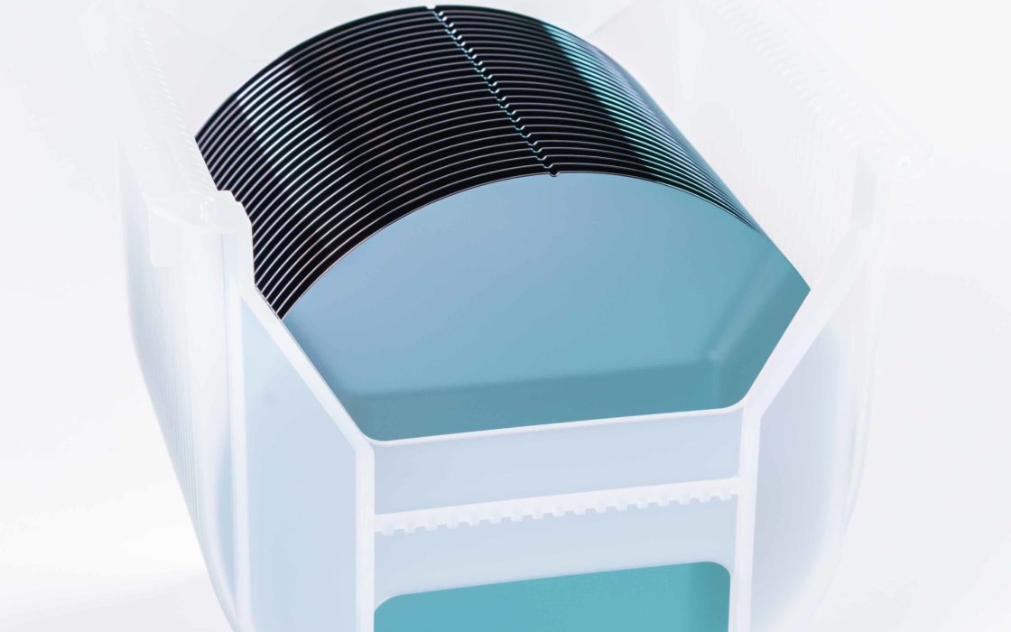
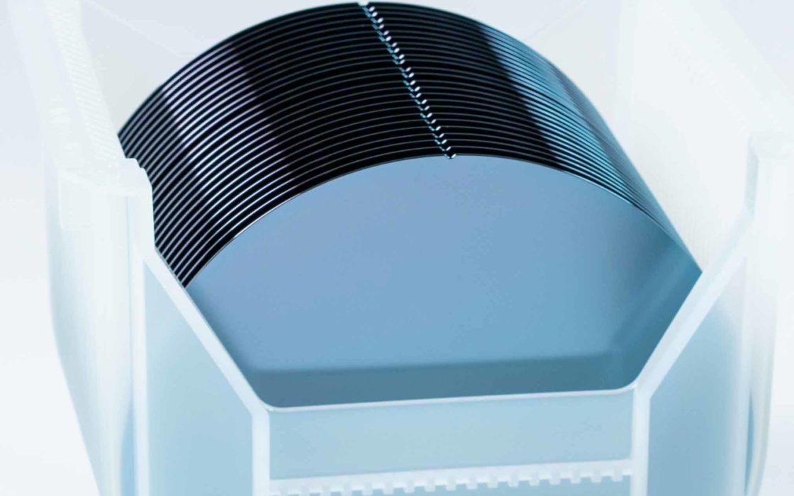
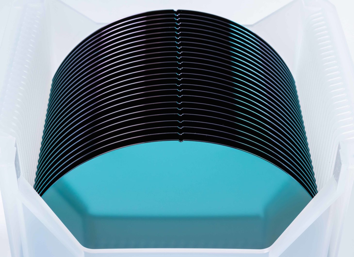
Okmetic High Resistivity Bonded SOI wafers with and without cavities are manufactured with Advanced Magnetic Czochralski (A-MCz®) crystal growth method enabling low Oi and very high resistivities of over 7,000 Ohm-cm. The SOI structure is made by bonding two silicon wafers together and leaving an insulating buried oxide layer between them. Typically mm wave devices are built on the top wafer acting as a device layer. The buried oxide layer is an excellent electric insulating layer and it also forms an effective etch-stop in device manufacturing. It can also act as a sacrificial layer when manufacturing more complex devices. The lower handle wafer is supporting the structure but can also be utilized in sealing the structure. Read more about Bonded SOI wafers and Cavity SOI wafers. High Resistivity SOI wafers are also available as Terrace Free SOI wafers providing maximized usable area.
High Resistivity BSOI wafer specifications
| Growth method | MCz, A-MCz® |
| Diameter | 150 mm, 200 mm |
| Crystal orientation | <100>, <111> |
| N type dopants | Phosphorus |
| P type dopants | Boron |
| Resistivity | Up to >7,000 Ohm-cm*, available also in Engineered Ultra High Resistivity version with 10 kOhm-cm resistivity *Resistivity range varies by dopant and orientation |
| Oxygen | Typically ≤5 ppma or ≤10 ppma (ASTM F121-83). Can be optimized to Customer process. |
| Device layer thickness | From 1 μm to >200 μm |
| Buried oxide layer thickness | From 0.3 μm to 4 μm, typically between 0.5 μm and 2 μm Type: Thermal oxide |
| Handle wafer thickness | 200 mm: 300 μm to 950 μm, typically 500-725 μm 150 mm: 300 μm to 950 μm, typically 380-675 μm |
| Back surface | Polished, etched |
| Terrace area | Standard or Terrace Free (Available for 200 mm) |
See all our 150-200 mm silicon wafers