MEMS and sensors
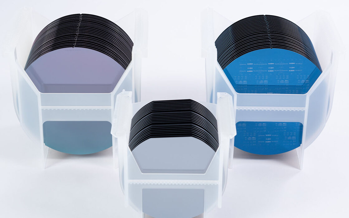
Silicon wafers have a great effect on device performance, Total Cost of Ownership and time to market. This is why device manufacturers are paying more attention to the choice of substrate and the demand for device and process optimized substrates is increasing.
Finding an optimal silicon wafer platform for one’s device and process needs isn’t always easy. To make the search easier we have compiled an indicative and non-exhaustive list of MEMS and sensor devices and suitable wafer options below. Our sales and technical support are happy to help you find a perfect silicon solution for your device and process needs.
Pressure sensors
There is a variety of platform options for pressure sensors such as SSP wafers, DSP wafers and entire line of Bonded SOI wafers or Wafers with built-in patterns. The latter two of which are highly beneficial for more advanced pressure sensor designs and they enable the manufacture of extremely small pressure sensors.
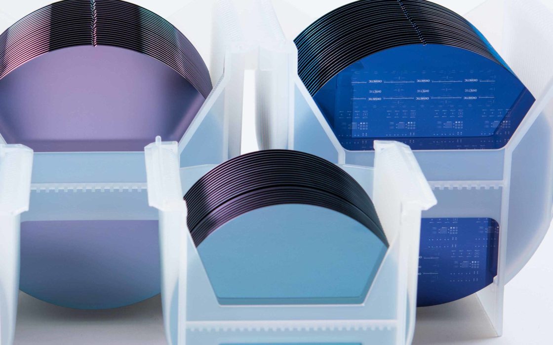
Okmetic Bonded SOI wafers are manufactured by bonding two silicon wafers together leaving an insulating buried oxide layer between them. Typically sensing elements are built on the top wafer acting as a device layer. The 0.3-SOI wafer is beneficial platform for pressure sensors due to its improved ±0.3 μm device layer thickness tolerance. In case tighter thickness tolerance is needed, E-SOI® is the answer with its thick and highly uniform device layer with a ±0.1 μm thickness tolerance. By using E-SOI® wafer as a pressure sensor platform one can achieve smaller die size, greatly reduced membrane thickness variation to maintain deflection variation window and improved device precision and/or greatly reduced device dimension as a result of precise layers. Both BSOI and E-SOI® wafers are also available as Terrace Free SOI wafers.
Turnkey, custom Wafers with built-in patterns and buried cavities (C-SOI®) enable more optimized pressure sensor manufacturing process flow and allow device makers to reallocate resources for more critical process steps and further processing of wafers for end applications. For example, Okmetic Cavity SOI (C-SOI®) wafers with thin membranes are widely used for pressure sensors as they enable more streamlined and cost-effective device manufacturing and more ambitious device designs with better performance.
MEMS based microfluidic devices, bio MEMS and flow sensors
There is a variety of platform options for microfluidic devices such as SSP wafers, DSP wafers and entire line of Bonded SOI wafers or Wafers with built-in patterns. The latter two of which are highly beneficial for more advanced designs.
Okmetic Bonded SOI wafers are ideal platform for microfluidic devices, bio MEMS and flow sensors. The BSOI wafers are manufactured by bonding two silicon wafers together leaving an insulating buried oxide layer between them. Typically sensing elements are built on the top wafer acting as a device layer. BSOI wafers have many benefits as they enable more ambitious device designs, improved device performance and smaller die size and they can be fully customized to meet your device and process needs.
Turnkey, custom Wafers with built-in patterns and buried cavities (C-SOI®) enable more optimized microfluidic device manufacturing process flow and allow device makers to reallocate resources for more critical process steps and further processing of wafers for end applications. Okmetic’s high-technology Cavity SOI (C-SOI®) wafer process enables the manufacture of extremely thin and thick membranes, which expands the variety of device design and processing possibilities. Depending on the design, both thin and thick membranes can be used for applications such as microfluidic devices like inkjet heads.
Transducers and actuators
There is a variety of platform options for transducers and actuators such as SSP wafers, DSP wafers, Wafers with built-in patterns and entire line of Bonded SOI wafers. Bonded Silicon-On-Insulator wafers offer advanced platform, which in many cases are more cost-effective choice than bulk silicon wafers. BSOI wafers have many benefits as they enable more ambitious device designs, improved device performance and smaller die size and they can be fully customized to meet your device and process needs.
MEMS cooling devices
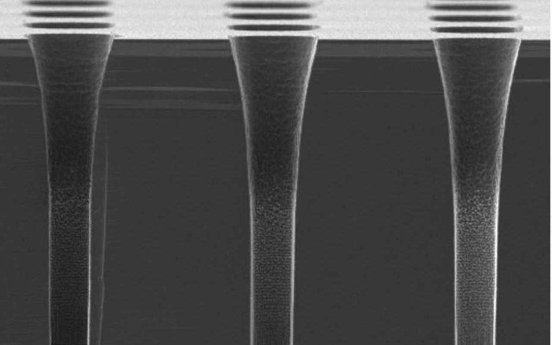
A range of advanced SOI platforms can be utilized for MEMS-based cooling devices, including Bonded SOI, Enhanced SOI, and C-SOI® wafers. These technologies provide an excellent foundation for cooling solutions based on micromechanical actuation and airflow generation. The highly uniform device layer thickness available with advanced SOI technologies enables optimized membrane structures and precise mechanical performance, supporting compact, high-performance cooling architectures. SOI-based platforms also offer extensive customization to meet specific device designs and manufacturing requirements.
Inertial sensors / accelerometers, gyroscopes and IMU’s
There is a variety of platform options for inertial sensors (accelerometers, gyroscopes and IMU’s) such as SSP wafers, DSP wafers and entire line of Bonded SOI wafers or Wafers with built-in patterns. The latter two of which are highly beneficial for more advanced inertial sensor designs.
Okmetic Bonded SOI wafer solutions are widely used in 3-axis accelerometers and gyroscopes. The BSOI wafers are manufactured by bonding two silicon wafers together leaving an insulating buried oxide layer between them. Typically sensing elements are built on the top wafer acting as a device layer. BSOI awafers are also available as Terrace Free SOI wafers.
Turnkey, custom Wafers with built-in patterns and buried cavities (C-SOI®) enable more optimized inertial sensor manufacturing process flow and allow device makers to reallocate resources for more critical process steps and further processing of wafers for end applications. Okmetic’s high-technology cavity SOI (C-SOI®) process enables the manufacture of extremely thin and thick membranes. Cavity SOI wafers with thicker membranes offer significant benefits for devices such as inertial sensors (gyroscopes, accelerometers, IMUs). Okmetic C-SOI® wafers pass the tightest quality standards as we have been supplying C-SOI® wafers for automotive inertial sensors since 2006.
Silicon speakers
Okmetic has been supplying Bonded SOI wafers for silicon speakers since 2006. In recent years, E-SOI® wafers’ usage in speakers has increased due to its unique properties: thick and highly uniform device layer with a ±0.1 μm thickness tolerance. E-SOI® wafer as a silicon speaker platform can achieve smaller die size, greatly reduced membrane thickness variation to maintain deflection variation window and improved device precision and/or greatly reduced device dimension as a result of precise layers.
Turnkey, custom Wafers with built-in patterns and buried cavities (C-SOI®) enable more optimized silicon speaker manufacturing process flow and allows device makers to reallocate resources for more critical process steps and further processing of wafers for end applications. Okmetic’s high-technology Cavity SOI (C-SOI®) wafer process enables the manufacture of extremely thin membranes, which are widely used in the manufacture of silicon-based speakers.
Silicon photonics, micromirrors and optical MEMS devices (MOEMS)
Silicon photonics, micromirrors and optical MEMS devices often benefit from the more advanced substrates.
BSOI wafers are one platform option for MOEMS ia. micro-optoelectromechanical systems. The BSOI wafers are manufactured by bonding two silicon wafers together leaving an insulating buried oxide layer between them.
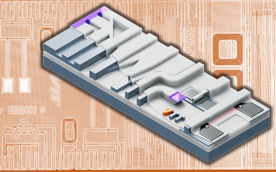
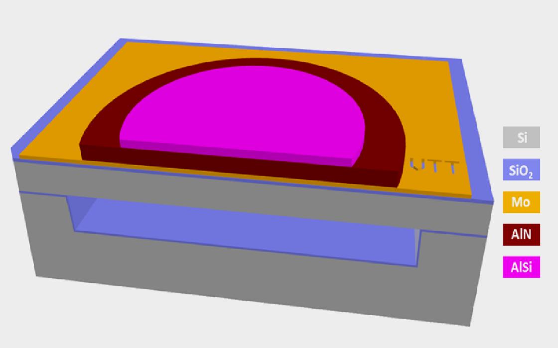
Okmetic’s E-SOI® wafer is an optimal platform for silicon photonics and optical MEMS devices due to its thick and highly uniform device layer enabling better performance and cost savings. Silicon photonics is a rapidly growing technology with applications such as optical transceivers, optical sensors and LiDAR systems. More advanced silicon photonic integrated circuits (PICs) can also use EC-SOI as a platform, which is a new technology platform combining E-SOI® and cavities. Okmetic has also co-operated with VTT to develop a highly beneficial platform for its Photonics technology. Read more about this from here.
Okmetic’s high-technology cavity SOI (C-SOI®) process enables the manufacture of extremely thin and thick membranes, which expands the variety of device design and processing possibilities. Cavity SOI wafers with thicker membranes offer significant benefits for devices such as micromirrors and other optical devices (like optical switches etc.).
MEMS oscillators and silicon timing devices
The use of highly doped ultra low resistivity wafers have expanded also to new application areas such as timing devices making silicon a viable option over quartz in Microelectromechanical system oscillators. The Low resistivity Bonded SOI wafers is found to be a beneficial platform to silicon-based oscillators as no external packaging is needed unlike with the quartz-based oscillators. This leads to reduced board size an absence of quality issues with external chips.
Okmetic E-SOI® wafer is also an ideal platform for demanding applications such as silicon timing devices due to its highly uniform device layer. E-SOI® enables increased design freedom, improved performance and precision and smaller die size.
Resonators
There is a variety of advanced platform options for resonators such as entire line of Bonded SOI wafers or Wafers with built-in patterns.
Okmetic Bonded SOI wafers are manufactured by bonding two silicon wafers together leaving an insulating buried oxide layer between them. Typically sensing elements are built on the top wafer acting as a device layer. The 0.3-SOI wafer is beneficial platform for resonators due to its improved ±0.3 μm device layer thickness tolerance. In case tighter thickness tolerance is needed, E-SOI® is the answer with its thick and highly uniform device layer with a ±0.1 μm thickness tolerance. E-SOI® as a resonator platform can achieve smaller die size, greatly reduced membrane thickness variation to maintain deflection variation window and improved device precision and/or greatly reduced device dimension as a result of precise layers. E-SOI® wafer has demonstrated to reduce frequency variation for resonant structures by 50% compared to epi-based SOI technology when using typical 7 µm device layer thickness for resonant structures. Both BSOI and E-SOI® wafers are also available as Terrace Free SOI wafers.
Turnkey, custom Wafers with built-in patterns and buried cavities (C-SOI®) enable more optimized resonator manufacturing process flow and allows device makers to reallocate resources for more critical process steps and further processing of wafers for end applications. Okmetic’s high-technology cavity SOI (C-SOI®) process enables the manufacture of extremely thin and thick membranes, which expands the variety of device design and processing possibilities. Depending on the design, both thin and thick membranes can be used for resonators and resonant structures.
Ultrasonic transducers like PMUT and CMUT
Okmetic’s high-technology cavity SOI (C-SOI®) process enables the manufacture of extremely thin membranes. Okmetic Cavity SOI wafers with thin membranes are widely used for ultrasonic transducers like Piezoelectric Micromachined Ultrasonic Transducers (PMUT) and Capacitive Micromachined Ultrasonic Transducers (CMUT) and ultrasonic sensors. Other beneficial platform option is EC-SOI, a combination of highly uniform E-SOI® wafer and cavities.
Also turnkey, custom Wafers with built-in patterns and buried cavities (C-SOI®) enable more optimized PMUT and CMUT manufacturing process flow and allows device makers to reallocate resources for more critical process steps and further processing of wafers for end applications.
Okmetic has collaborated with VTT to enhance PMUT performance using C-SOI® and EC-SOI wafers. Read more about the collaboration here.
IC and MEMS process integrations
Okmetic’s high-technology Cavity SOI (C-SOI®) process enables the manufacture of extremely thin and thick membranes. Depending on the design, both thin and thick membranes can be used for IC and MEMS process integrations.
CAP wafers
Turnkey, custom Wafers with built-in patterns and buried cavities (C-SOI®) can be used as a CAP wafer. Okmetic’s patterned wafers streamline the device manufacturing process flow and allow device makers to reallocate resources for more critical process steps and further processing of wafers for end applications.