Discrete Power Device wafers
Discrete Power Device wafers offer customizable resistivity from <0.001 to >1,500 Ohm-cm, restrained resistivity spread, optimized oxygen concentration and low defect density. MCz and A-MCz® crystal growth methods, along with a wide selection of wafer parameters, ensure customized, high-value-added wafer solutions with increased yield and breakdown voltage.
For decades, Okmetic has been a trusted supplier of Discrete Power Device wafers, establishing itself as a key player in the automotive industry since the 1990s. Our profound expertise in crystal growth, combined with our ability to deliver large volumes of customized wafer solutions, highlights our prominence in this sector.
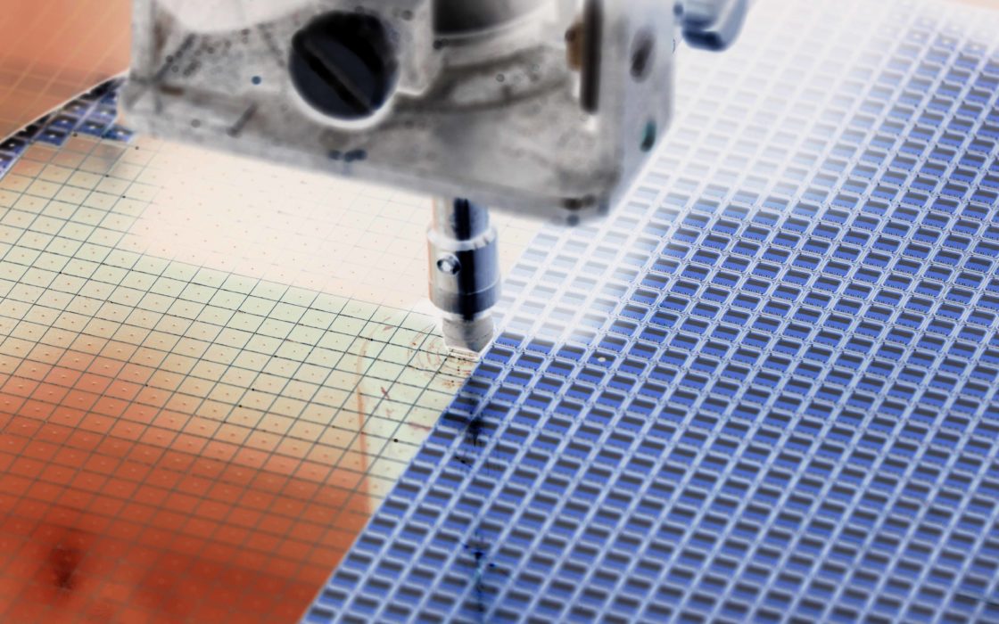
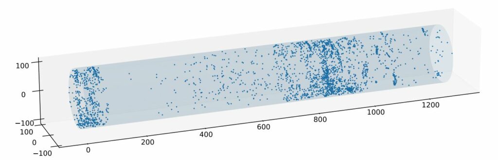
Increasing complexity of power devices and the expected gradual industry shift towards 300 mm Cz wafers will also place stricter requirements for 200 mm wafers. Okmetic Discrete Power Device wafers with customizable resistivity, tightly managed resistivity variation, fine-tuned oxygen concentration and low defect density enable extremely high-performing discrete power devices with increased yield. Okmetic has substantial expertise in minimizing crystal defects that impact the breakdown voltage of power devices. Our wafers are intricately engineered to be free from dislocations and slips, and feature optional COP level management for enhanced gate oxide integrity (GOI). Read more about Okmetic Low COP wafers. Okmetic also supplies EPI wafers.
Discrete Power Device wafers are intricately engineered to be free from dislocations and slips, and feature optional COP level management for enhanced gate oxide integrity.
Okmetic Discrete Power Device wafers can serve as drop-in replacements for FZ wafers in NPT/FS IGBT applications, or as substrates for challenging epitaxial deposition needed in PT IGBT, Power MOSFETs, HV Diodes, FRDs, SBDs, thyristors, power BJTs, and other bipolar devices.
Cost-efficient and high-performing alternative to FZ wafers
New MCz crystal growing methods have made Cz based silicon into the substrate of choice over FZ wafers. Okmetic Discrete Power Device wafers grown with MCz and A-MCz® crystal growth method provide a cost-efficient alternative to FZ silicon wafers for advanced NPT/FS IGBT devices. We can address issues commonly associated with Czochralski crystal growth method by optimized oxygen concentration, restrained resistivity spread and enhanced gate oxide integrity (GOI).
Okmetic Discrete Power Device wafers grown with MCz and A-MCz® crystal growth method provide a cost-efficient alternative to FZ silicon wafers for advanced NPT/FS IGBT devices.
Optimized oxygen concentration
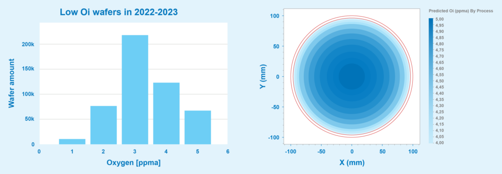
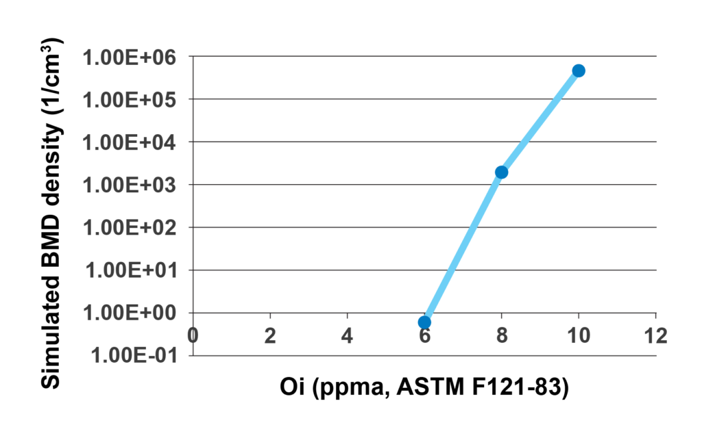
A reproducible low oxygen concentration (Oi) level can be guaranteed in high-volume production with the A-MCz® crystal growth method. The low Oi level (<5.5 ppma) minimizes thermal donor (TD) issues and suppresses Bulk Micro Defects (BMDs). Furthermore, optimized oxygen levels reduce the formation of oxygen-carbon complexes that can cause defects during IGBT annealing and high-energy implantation processes. To ensure thermal donor robustness, all wafers undergo a TD-killing process. Low Oi wafers do not suffer from defects caused by high oxygen concentration but still benefit from oxygen’s strengthening effect. This results in improved slip and radiation robustness compared to FZ wafers.
The low Oi level (<5.5 ppma) minimizes thermal donor (TD) issues and suppresses Bulk Micro Defects (BMDs).
Restrained resistivity spread
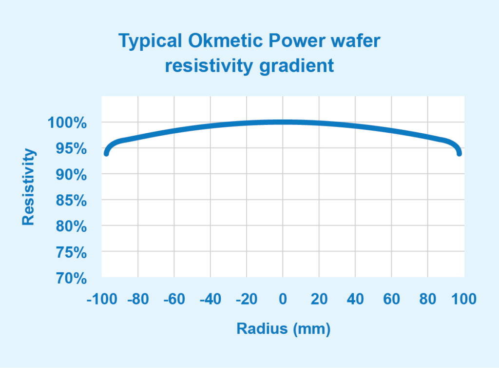
Discrete power device wafers demonstrate excellent resistivity uniformity across the wafer, with RRG typically below 8%. Okmetic has extensive experience in manufacturing higher resistivity wafers, 1,500 Ohm-cm or more, to meet the needs of the most demanding power devices. Resistivity tolerance is determined based on the price target and desired resistivity range.
Enhanced GOI performance
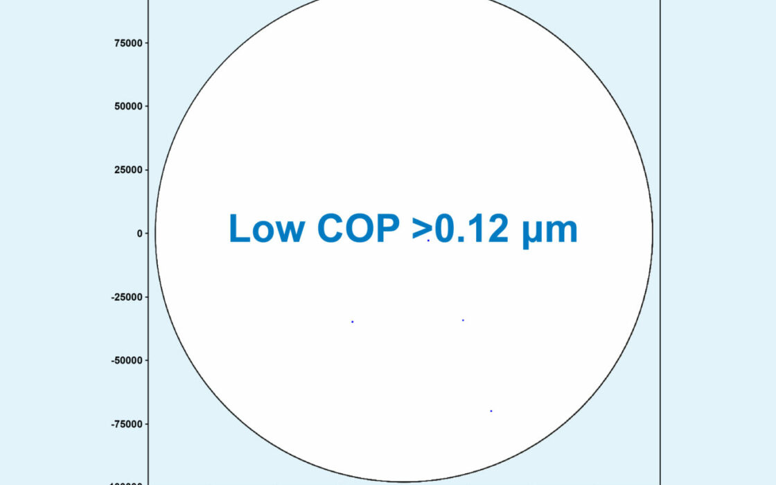
Okmetic also provides Low COP capability for enhanced Gate Oxide Integrity (GOI) performance. The GOI performance can be further enhanced by combining the low COP option to BMD optimized low Oi A-MCz® crystal growth method.
The GOI performance can be further enhanced by combining the low COP option to BMD optimized low Oi A-MCz® crystal growth method.
Customized epi-substrates for high quality epitaxy
Customized wafers in high volume manufacturing are the core of our business. We specialize in tailoring wafer parameters to meet the needs of even the most demanding power devices. Resistivities can be customized from very low to extremely high, ranging from 0.001 to >1,500 Ohm-cm, while wafer thickness can be customized to match our customers’ processes, spanning from 380 up to 1,150 µm. Additionally, Okmetic patterning capability enables superjunction and other modern trench structures.
Okmetic excels in LTO backsealing used for autodoping prevention and polyback sealing used for effective gettering. Moreover, we offer various combinations of LTO and Poly stacks, including Poly-LTO-Poly supersealing, to mitigate nodules and edge-related epi issues. Our customer support is happy to introduce different options for wafer warp/bow and resistivity window optimization to ensure misfit-free epi layers and predictable dopant/metal diffusion behavior. Additionally, our capabilities extend to wafer edge refining to meet the needs of even the most demanding processes such as wafer thinning and ultra-thick epitaxial deposition.
We offer various combinations of LTO and Poly stacks, including Poly-LTO-Poly supersealing, to mitigate nodules and edge-related epi issues.
Discrete Power Device wafer specifications
| Growth method | Cz, MCz, A-MCz® |
| Diameter | 200 mm, 150 mm |
| Crystal orientation | <100>, <110>, <111> |
| N type dopants | Antimony, Arsenic, Phosphorus, Red Phosphorus |
| P type dopants | Boron |
| Resistivity1 | Between <0.001 and >1,500 Ohm-cm |
| Resistivity tolerance | Determined per price target and resistivity range |
| Radial resistivity gradient (RRG)2 | Typically below 8% |
| Oxygen concentration (Oi)3 | <4 to 20 ppma |
| Radial oxygen gradient (ROG)4 | Typically below 10% |
| Carbon concentration5 | <0.5 ppma |
| SSP wafer thickness6 | 200 mm: 550 to 1,150 µm 150 mm: 400 to 1,150 µm |
| DSP wafer thickness6 | 200 mm: 380 to 1,150 µm 150 mm: 380 to >1,150 µm |
| SSP backside treatment | Etched, Polyback, LTO |
| COP amount7 | Standard or Low COP (depends on wafer size and resistivity) |
2SEMI MF84, depends on the resistivity target and edge exclusion
3ASTM F121-831/SEMI MF1188-1107
4SEMI MF951, low Oi: ROG >20%
5ASTM F123-91, limited by measurement technology
6Other thicknesses possible with certain limitations.
7Low COP available in 200 mm with certain limitations.
Fully CMOS compatible wafer surface quality and cleanliness requirements
See all 150-200 mm silicon wafers