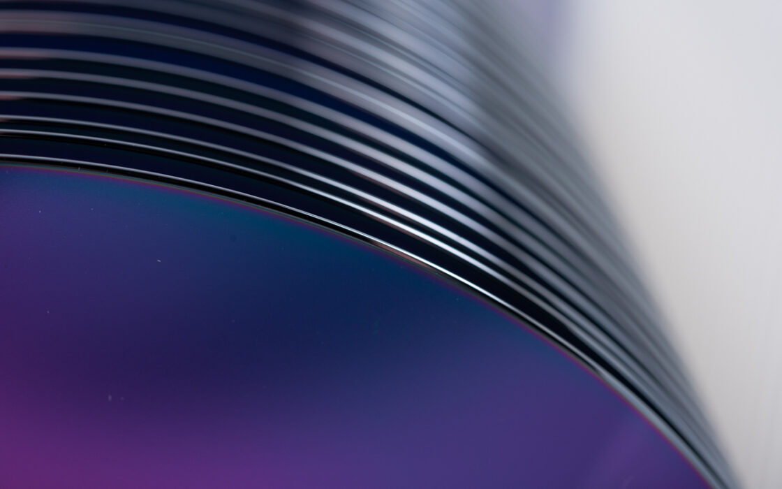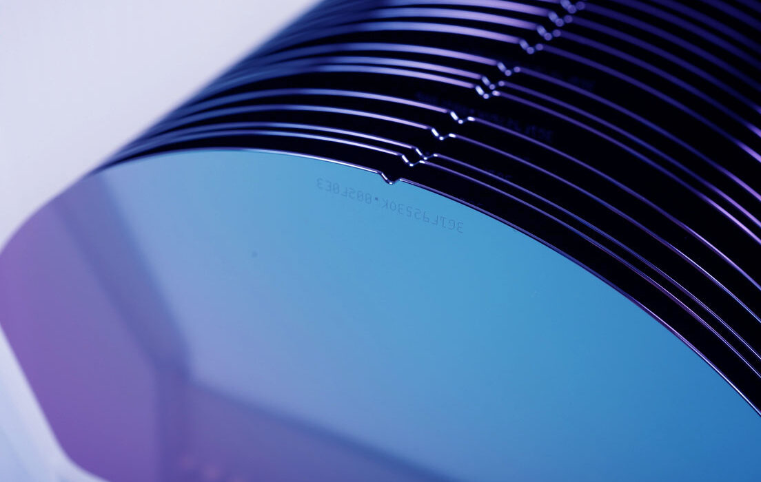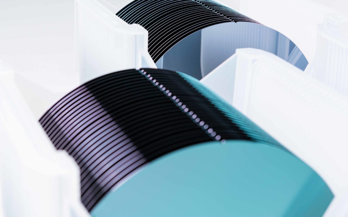
Power wafer line
Okmetic Power wafer line provides an optimal platform for the manufacture of various power devices. Our power device optimized wafer solutions improve power device performance, reduce Total Cost of Ownership and enable more refined designs.
Okmetic has been supplying wafers for power devices for decades. Wafers targeted for discrete power devices have been in the portfolio since the 1990’s whilst Power GaN Substrate wafers and Power Management SOI wafers were first introduced in the 2010’s. Power wafers’ capabilities are developed continuously in collaboration with customers. Okmetic power wafers enable the manufacture of power devices used in renewable energy solutions, electric cars, portable consumer products, as well as different solutions related to power management and efficiency improvement.
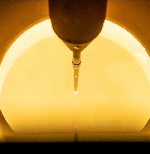
Okmetic’s power device optimized wafers are mainly manufactured with our signature Advanced Magnetic Czochralski (A-MCz®) crystal growth method, which coupled with wide selection of wafer parameters guarantee customized, high value-added wafer solutions with reduced power losses.
Line of power device optimized wafers
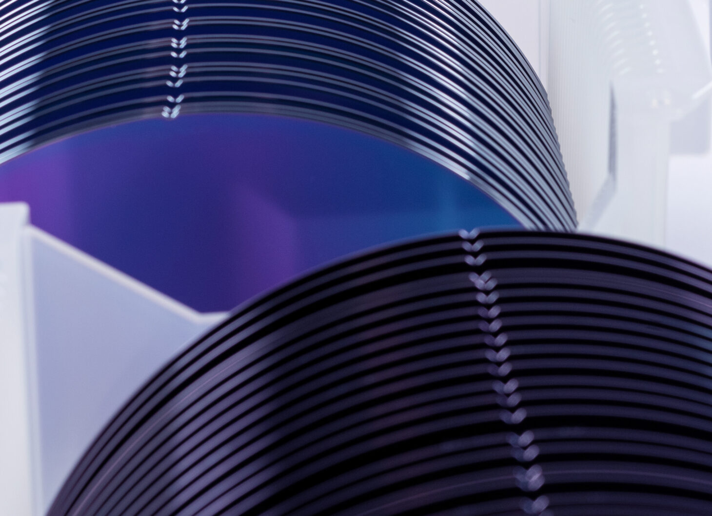
Okmetic power wafer line consists of specialty wafers with resistivities varying between <0.001 and >1,500 Ohm-cm. Different wafer types include 150 to 200 mm SSP, DSP and SOI wafers. Wafer resistivity, crystal orientation, oxygen content, COP levels and thickness can be customized to match your device or process needs. Okmetic provides wide range of wafer thicknesses from 380 to 1,150 μm. In mixed metal lattices like GaN epi layers, thicker wafers endure the extreme stresses of the epitaxial processes. Our sales and technical support are happy to help finding the optimal solution, customized for your needs.
Okmetic Power wafer line comprise:
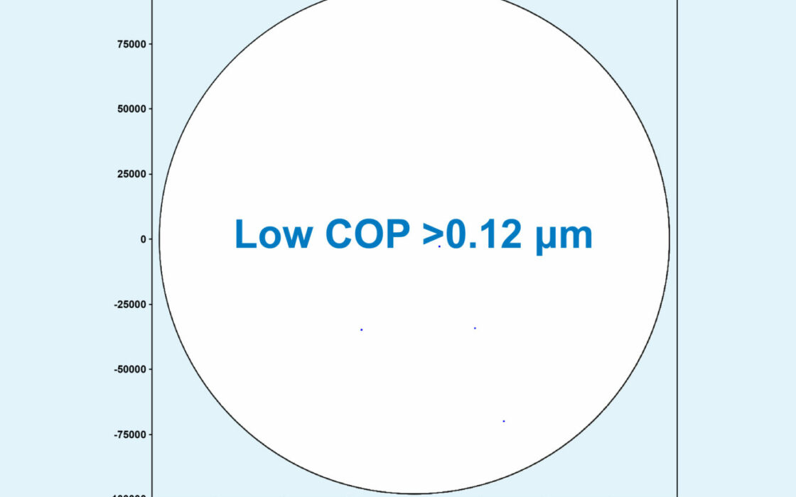
- Low COP capability for Discrete Power Device wafers and Power Management SOI wafers
- Silicon EPI wafers
White papers
A-MCz® crystal growth method benefits
1. Good availability in 150-200 mm
2. Availability in <111> orientation
3. Optimized Oi range to increase wafer strength at customer process. Less prone to slip and breakage.
4. Low COP capability
General SSP and DSP wafer specifications for Power semiconductors
| Growth method | Cz, MCz, A-MCz® |
| Diameter | 200 mm, 150 mm |
| Crystal orientation | <100>, <110>, <111> |
| N type dopants | Antimony, Arsenic, Phosphorus, Red Phosphorus |
| P type dopants | Boron |
| Resistivity1 | Between <0.001 and >1,500 Ohm-cm |
| Resistivity tolerance | Determined per price target and resistivity range |
| Radial resistivity gradient (RRG)2 | Typically below 8% |
| Oxygen concentration (Oi)3 | <4 to 20 ppma |
| Radial oxygen gradient (ROG)4 | Typically below 10% |
| Carbon concentration5 | <0.5 ppma |
| SSP wafer thickness6 | 200 mm: 550 to 1,150 µm 150 mm: 400 to 1,150 µm |
| DSP wafer thickness6 | 200 mm: 380 to 1,150 µm 150 mm: 380 to >1,150 µm |
| SSP backside treatment | Etched, Polyback, LTO |
| COP amount7 | Standard or Low COP (depends on wafer size and resistivity) |
2SEMI MF84, depends on the resistivity target and edge exclusion
3ASTM F121-831/SEMI MF1188-1107
4SEMI MF951, low Oi: ROG >20%
5ASTM F123-91, limited by measurement technology
6Other thicknesses possible with certain limitations.
7Available in 200 mm with certain limitations.
Fully CMOS compatible wafer surface quality and cleanliness requirements
General SOI wafer specifications for Power semiconductors
| Growth method | Cz, MCz, A-MCz® |
| Diameter | 200 mm, 150 mm |
| Crystal orientation | <100>, <111> |
| N type dopants | Phosphorus, Red Phosphorus, Antimony, Arsenic |
| P type dopants | Boron |
| Resistivity1 | <0.001 to >1,500 Ohm-cm |
| Resistivity tolerance | Determined per price target and resistivity range |
| Oxygen concentration (Oi)2 | <4 to 13 ppma |
| Device layer thickness3 | 1 μm to >200 μm (±0.1 µm) |
| Buried oxide layer thickness4 | 0.3 μm to >5 μm |
| Handle wafer thickness5 | 300 μm to 950 μm (±3-5 µm) |
| Back surface | Polished, etched, oxide or without oxide |
| COP amount6 | Standard or Low COP (depends on wafer size and resistivity) Zero COP SOI available with annealing process |
| Terrace area | Standard or Terrace Free (Available in 200 mm) |
2ASTM F121-831/SEMI MF1188-1107
3Other thicknesses possible with certain limitations. 150mm tolerance ±0.2 µm
4Type: thermal oxide. Typically 0.5 μm to 2 μm, >5 μm BOX possible with certain limitations
5 200 mm: typically 725 μm, 150 mm: typically 675 μm,±3 µm tolerance for demanding devices
6 Available in 200 mm with certain limitations.
Fully CMOS compatible wafer surface quality and cleanliness requirements
See all 150-200 mm silicon wafers
Contact us
Request a quote or product details
Application areas
- Power MOSFETs
- IGBTs
- Schottky and power diodes
- Power BJTs
- Thyristors
- CMOS and BiCMOS manufactured devices
- Smart power / BCD and lateral HV devices
- Battery and Power Management ICs
- Intelligent power modules
- Other Smart Power applications using advanced BCD or BiCMOS processes
- GaN HEMT devices
- High power LEDs
- Monolithic all GaN integration
- And more..