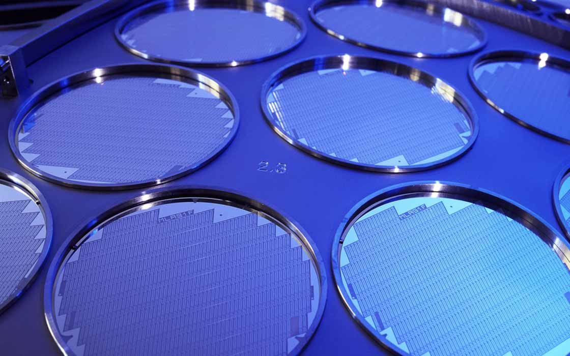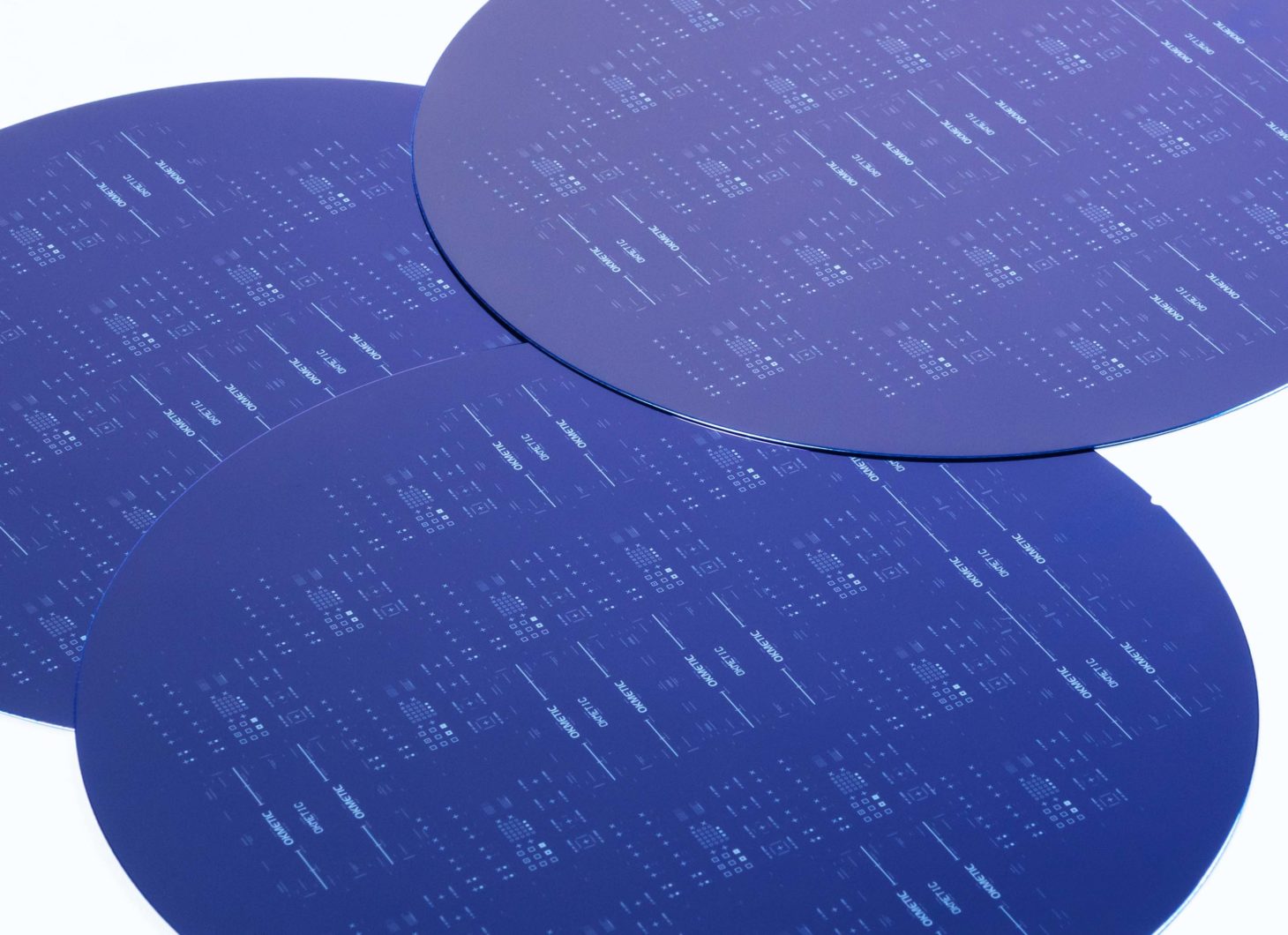
Patterned wafers – DRIE and Lithography
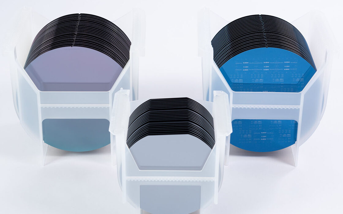
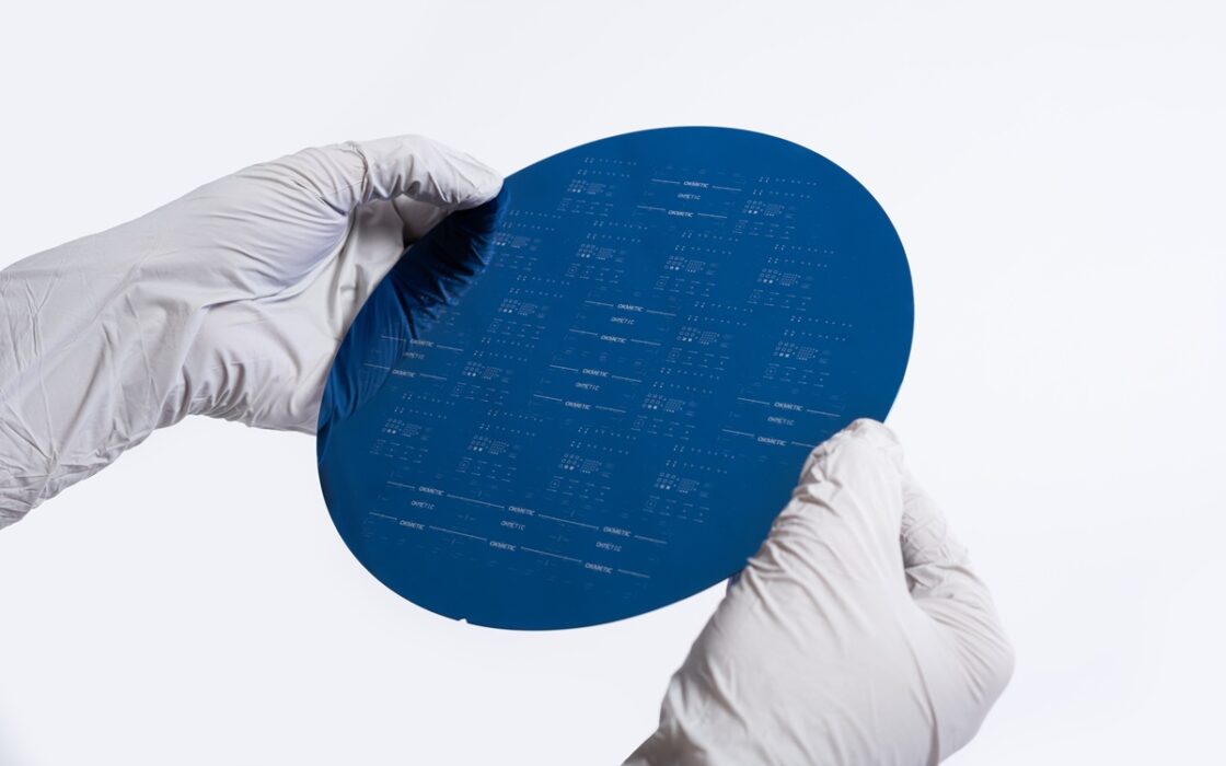
Okmetic SSP, DSP and SOI wafers with built-in patterns and buried cavities (C-SOI®) enable more optimized MEMS and RF manufacturing. Fully in-house process covering crystal growth, wafering, lithography, DRIE and fusion bonded SOI guarantee supreme quality and shorter time-to-market.
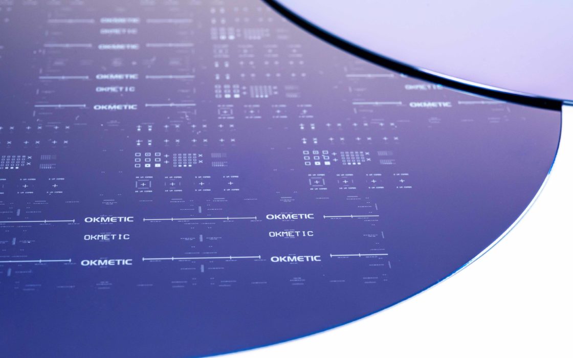
There is increasing demand towards turnkey, custom wafers and tailored wafer structures in the MEMS and RF device market. Okmetic’s SSP, DSP and SOI wafers with built-in patterns and cavities (C-SOI®) are customized to match customer device design and process seamlessly and they are manufactured fully in-house at Okmetic. This increases wafer quality and reliability significantly in addition to enabling more ambitious device designs and shorter time-to-market. The patterned wafers’ quality and cleanliness standards are identical with bulk silicon wafers.
Silicon wafers with built-in patterns optimize MEMS and RF processing as they are customized to match customer device design and process seamlessly
These kinds of more ready-made substrates create true value for the device manufacturer as they remove process steps making the MEMS or RF process less complex and allow manufacturers to save their own capacity and focus on other more critical process steps.
Patterning is an additional process step enabling more streamlined and easy manufacture of pressure sensors, silicon microphones, microfluidic devices like inkjet heads, inertial sensors, IC and MEMS process integrations, ultrasonic transducers like PMUT and CMUT’s, micromirrors and other optical devices, timing devices and other resonators and CAP wafers.
Device design taken into account at all wafer processing steps
In order to have better performing devices and more optimized processes, wafers and their parameters must be customized for device and process needs. Also with SSP, DSP and SOI wafers with built-in patterns and buried cavities the customer device design and process create the basis for Okmetic’s wafer design and processing. The customer device design and process is taken into account at every step of the wafer processing: crystal growth, wafering, SOI processing, lithographic patterning and deep reactive-ion etching (DRIE).
Superior quality compared to process of reference
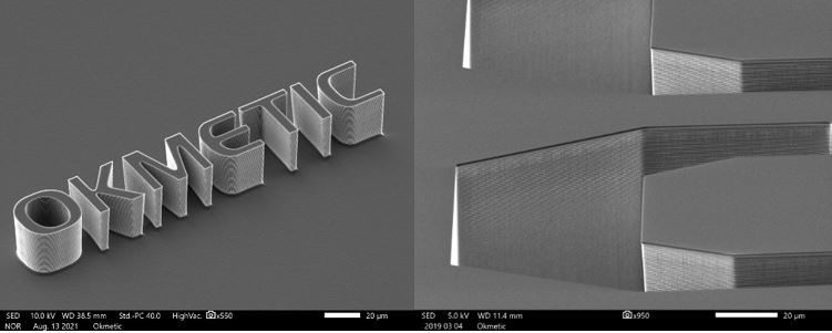
One key factor for high-performance wafers is the state-of-the-art manufacturing process and vast expertise. Okmetic’s few years old patterning line was designed for this purpose only which can be seen in superior wafer quality and reliability. When examining die yield, Okmetic’s patterning process is clearly better than process of reference in AVI defectivity. Also, the DRIE process showcases superior uniformity when etching shallow cavities and deep or complicated structures, which can be seen in better performance and higher precision of customer devices.
Superior uniformity when etching shallow cavities and deep or complicated structures
The tools and processes of patterning line are designed for defectless cavities and surfaces
- Automated wafer and vacuum back surface handling
- Through wafer IR alignment capability making backside alignment marks redundant
- Wafer level traceability with integrated laser code readers
- Minimized wafer exposure to ambient air between the etching steps
- Improved AVI and bonding defectivity inspection
Excellent etching accuracy
- The option for vertical sidewalls
- High etching rate and effective etch stop
- Predictable and consistent bulk behavior in etching
- Excellent accuracy and uniformity of the etched structures
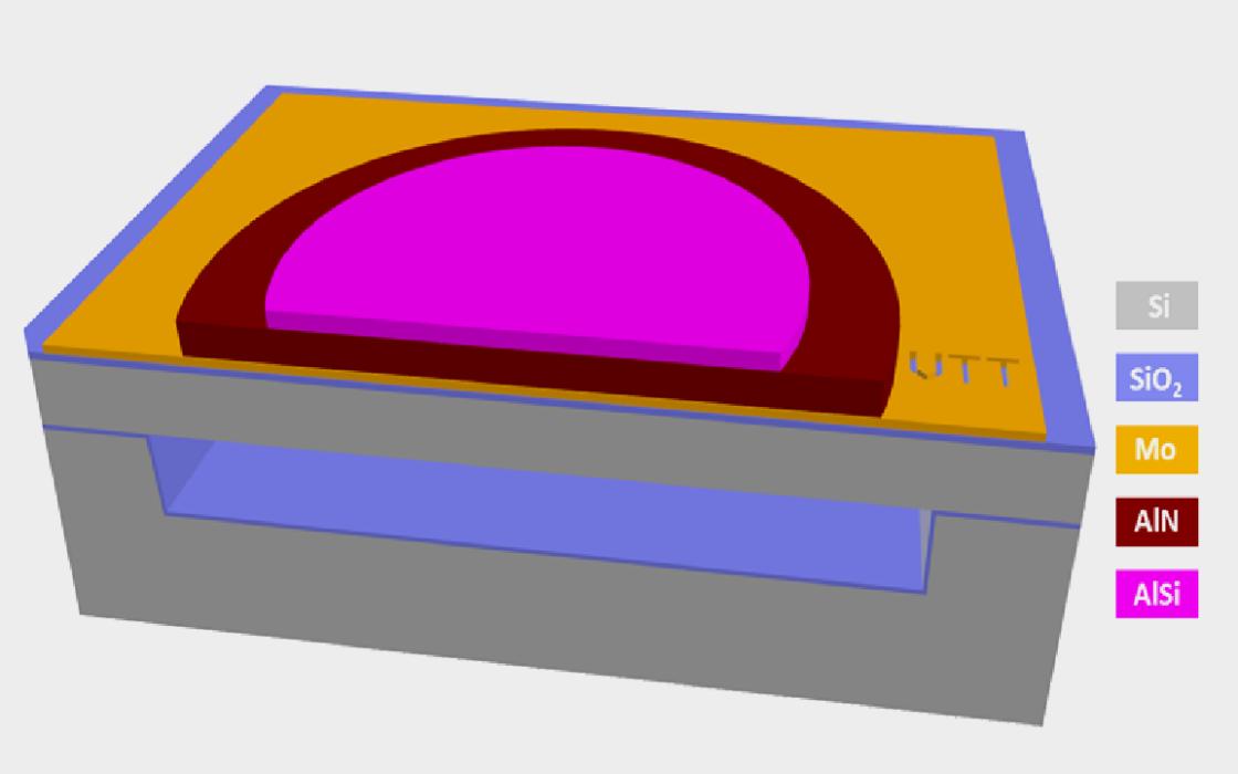
How are wafers with built-in patterns manufactured
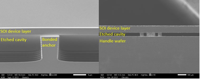
When manufacturing silicon wafers with built-in patterns and cavities a mask oxide is grown for protection of wafer surface during patterning steps. Wafer surface is then coated with photosensitive material. Desired areas of resist are exposed with UV light followed by development and etching. Patterned features such as cavities and device membranes are inspected for defectivity with automated inspection tool. Cap wafer is bonded on top of the wafer with built-in patterns and thinned down to desired thickness to create a C-SOI® wafer. Bonded interface is inspected for defectivity with an ultrasound. C-SOI® wafer is patterned to create electrical feedthroughs through the top layer.
New patterning line in use since 2019

Okmetic’s decades-long crystal growth, wafering and SOI expertise was complimented with lithographic patterning and deep reactive-ion etching (DRIE) capability during 2017 and 2018. At the same time, the Vantaa plant was expanded with over 1,000 m2 of additional clean room space and a new line dedicated entirely for the patterning of SSP, DSP and SOI wafers. The first volume orders from the new patterning line were delivered in February 2019. Before the new line, the patterning service was outsourced during years 2005-2018.
C-SOI® wafer specifications
The tables below give some guidelines on Okmetic C-SOI® wafer specifications. Our C-SOI® wafers are always customized solutions, so please contact our sales and technical support for more detailed information.
| C-SOI® wafer diameter | 150 mm, 200 mm |
Device layer specifications
| Growth method | Cz, MCz, A-MCz® |
| Crystal orientation | <100>, <110>, <111> |
| N type dopants | Antimony, Phosphorus |
| P type dopants | Boron |
| Resistivity | From <0.001 to >7,000 Ohm-cm* *Resistivity range varies by dopant and orientation |
| Device layer / membrane thickness | From 2 μm to >200 μm |
| Device layer / membrane thickness tolerance | Typically ±0.5 μm, down to ±0.2 μm with EC-SOI |
Buried oxide (BOX) specifications
| Type | Thermal oxide grown on handle or device wafer or both |
| Thickness | From 0.3 μm to 5 μm, typically between 0.5 μm and 2 μm |
Handle wafer specifications
| Growth method | Cz, MCz, A-MCz® |
| Crystal orientation | <100>, <110>, <111> |
| N type dopants | Antimony, Phosphorus |
| P type dopants | Boron |
| Resistivity | From <0.001 to >7,000 Ohm-cm* *Resistivity range varies by dopant and orientation |
| Handle wafer thickness | 200 mm: 380 μm to 675 μm 150 mm: 380 μm to 725 μm |
| Handle wafer thickness tolerance | ±5 μm |
| Back surface | Polished or etched with oxide |
Cavity specifications
| Cavity location | Handle wafer or device layer, or buried oxide |
| Cavity depth (in silicon) | 2 – 500 µm |
| Minimum CD | 2 µm |
| Max cavity span length vs. membrane thickness | <40:1 µm with standard C-SOI® process |
Front surface alignment marks
| Alignment accuracy, buried cavity to front surface alignment marks | ±1 µm |
| Mark design | Customer tool specific |