TSV wafers – Through Silicon Vias
Okmetic TSV wafers with pre-formed blind vias enable compact 3D MEMS integration and advanced wafer-level packaging. TSV structures are available on DSP, Bonded SOI, and C-SOI® wafer platforms for a wide range of MEMS and packaging applications. The vias can be supplied as polysilicon-filled or unfilled structures with optional thermal oxide insulation according to integration requirements.
Okmetic TSV wafers enable isolated electrical connections through silicon wafers, supporting reduced die size, interlayer connectivity, and compact 3D MEMS integration. Available on Double Side Polished (DSP) silicon wafers as well as Bonded SOI and C-SOI® wafer platforms, Okmetic TSV wafers are used as interposers and capping wafers in a variety of MEMS and sensor applications such as resonators and inertial sensors. The wafers also support wafer-level packaging and emerging applications, including quantum devices.
Okmetic TSV wafers help reduce the die size of MEMS devices and enable interlayer connectivity and 3D MEMS integration
TSV wafer processing and blind via structures
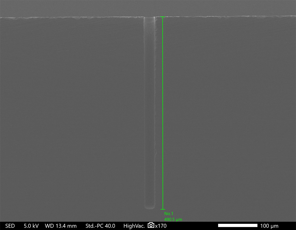
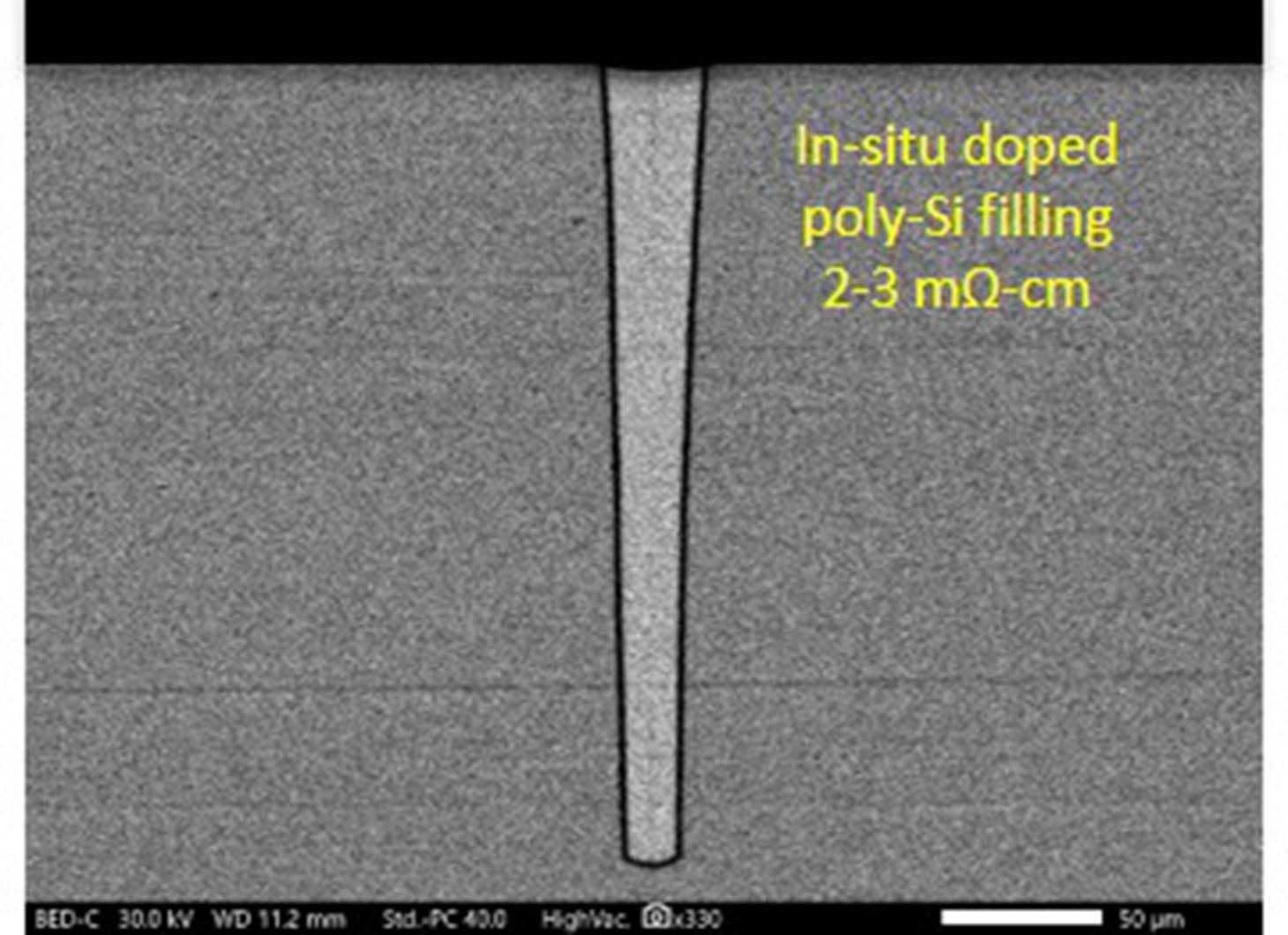
Okmetic TSV wafers are manufactured using a Via-First approach compatible with advanced MEMS manufacturing processes. Blind vias are plasma-etched into DSP wafers and are available with in-situ boron-doped polysilicon filling, undoped poly-Si filling, or as unfilled structures depending on customer integration requirements. The unfilled option allows device manufacturers to fill the vias according to their specific process requirements. Optional thermal oxide insulation enables electrically isolated vertical interconnects. Blind vias are revealed later during wafer thinning or back grinding at the device manufacturer.
By shifting critical via processing upstream, device manufacturers can simplify subsequent processing and reduce overall process complexity.
The TSV process flow includes:
- Blind via etching (DRIE)
- Optional thermal oxide insulation
- Optional polysilicon filling
- Field poly-Si removal
- Customer thinning and via reveal
Blind vias are available in stadium-shaped and circular geometries. Stadium-shaped blind vias support aspect ratios up to approximately 20:1, while circular blind vias support aspect ratios up to approximately 15:1 depending on via design and filling requirements.
TSV wafers are compatible with standard anodic, metal, and glass frit bonding methods commonly used in downstream MEMS manufacturing and wafer-level packaging processes.
TSV structures on SOI and C-SOI® wafers
Okmetic offers TSV structures on Bonded SOI and C-SOI® wafer platforms for advanced MEMS integration and wafer-level assembly. Combining TSV structures with SOI-based wafer platforms enables compact bonded MEMS structures and supports advanced MEMS device architectures.
In Bonded SOI and C-SOI® structures, poly-filled blind vias or plugs through the SOI device layer enable vertical electrical interconnects and are implemented without electrical insulation. Unfilled blind vias can also be implemented in the handle layer depending on the integration architecture and downstream processing requirements.
Combining TSV wafers with C-SOI® wafers enables simplified wafer-level packaging, reduced die size, heterogeneous device integration, and cost-effective capping and assembly processes.
Demonstrated performance in MEMS devices
Okmetic TSV wafers with polysilicon filling are compatible with high-temperature processes and their cleanliness fully meets CMOS manufacturing standards. Poly-Si vias are robust and easy to integrate since they only consist of silicon and thermal SiO₂ with well-known material properties. After via reveal, customers can use well-established metallic interconnections and bumps for backside integration and electrical connection to poly-TSVs.
Okmetic TSV structures have demonstrated excellent electrical performance in MEMS devices with uniform resistivity, low via resistance, low capacitance, and very low leakage current.
- Resistivity uniformity <5% wafer to wafer and within wafer
- Resistance 10-15 Ohm (30 µm diameter, 200 µm depth)
- Capacitance <0.5 pF (2 µm thermal oxide insulation)
- Leakage current <0.5 pA@100 V (2 µm thermal oxide)
High-quality TSV wafers and technical support
Okmetic TSV wafers are manufactured on high-quality silicon wafer platforms featuring excellent thickness uniformity, orientation accuracy, crystal quality, and homogeneity. Our TSV wafers fully meet CMOS manufacturing requirements for impurity and surface quality levels.
Our sales and technical support teams work closely with customers to optimize TSV wafer structures according to integration and packaging requirements, including wafer thickness, via geometry, via density, aspect ratio, resistivity, capacitance, isolation performance, and wafer bonding compatibility.
DSP wafers used for TSV, specifications
| Growth method | Cz, MCz, A-MCz® |
| Diameter | 200 mm, 150 mm |
| Crystal orientation | <100>, <110>,<111>, off-oriented |
| N type dopants | Antimony, Phosphorus, Red Phosphorus |
| P type dopants | Boron |
| Resistivity1 | From <0.001 to >7,000 Ohm-cm |
| Thickness2 | 600 to 1,150 μm |
| Thickness tolerance3 | ±5 µm |
| TTV | <1 μm or ≤0.7 μm |
| DSP orientation accuracy4 | ±0.2° |
| SFQR | ≤0.2 μm |
2Other thicknesses possible with certain limitations.
3±3 µm for demanding devices.
4±0.15° for demanding devices.
Full CMOS compatible metal impurity and surface quality levels
TSV design aspects
| Width | 7-30 µm |
| Length | >2x width |
| Depth | <250 µm |
| Aspect ratio | <10 |
| Via density | <20 vias/mm2 |
| Isolation oxide thickness | 0.5…2.0 µm |
| Via dishing | <0.5 µm |
| Via resistivity | <5 mOhm-cm (In-situ boron-doped polysilicon) |