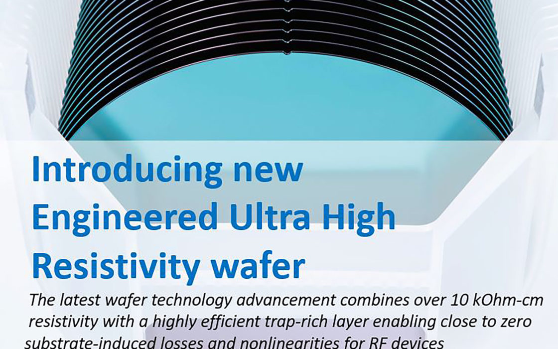
Engineered Ultra High Resistivity wafers
Okmetic Engineered Ultra High Resistivity SSP and DSP wafers combining over 10,000 Ohm-cm resistivity with highly efficient trap-rich layer enable close to zero substrate-induced losses and nonlinearities of RF devices. These premium wafers are optimized to meet the most demanding RF filter needs.
Okmetic Engineered Ultra High Resistivity wafers are premium silicon substrates with maximum performance, optimized for demanding radio frequency filter and device needs. The Engineered Ultra High Resistivity wafers boast with over 10,000 Ohm-cm of bulk resistivities, low Oi and highly efficient trap-rich layer.
This most advanced wafer technology leverages Okmetic’s proprietary Advanced Magnetic Czochralski (A-MCz®) crystal growth process to deliver highest resistivity and best technical performance in the form of close to zero substrate-induced losses and nonlinearities for RF devices. Find out more about our Engineered high resistivity wafer benefits in our White paper “Advancing from 4G LTE to 5G and 6G: Engineered RFSi® silicon wafers for high-performance RF devices.
Engineered Ultra High Resistivity wafers deliver highest resistivity and best technical performance in the form of close to zero substrate-induced losses and nonlinearities
Optimized for demanding RF filter and device needs
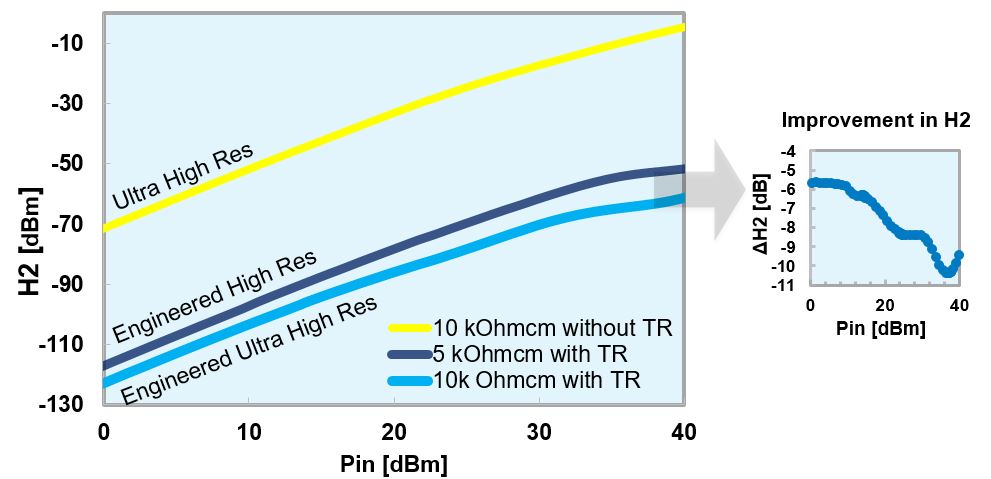
Engineered Ultra High Resistivity wafers are optimized for demanding RF filter and device needs and they aim to facilitate the RF device design and modelling. The Engineered Ultra High Resistivity wafers offer highest effective resistivity, close to zero substrate-induced losses and nonlinearities as well as superior 2nd harmonic and intermodular distortion (IMD) values. Engineered Ultra High Resistivity wafers enable RF filters to reach very low second harmonic levels of <-90 dBm measured at 900 MHz fundamental tone and extremely low IMD3 levels of even <-105 dBm.
Engineered Ultra High Resistivity wafers enable RF filters to reach very low second harmonic levels of <-90 dBm measured at 900 MHz fundamental tone and extremely low IMD3 levels of even < -105 dBm.
Another advantage of Ultra High Resistivity wafers is that their oxygen content is optimized. This improves wafer strength and makes them a more robust option for ultra high resistivity FZ wafers. Engineered Ultra High Resistivity wafers are typically used in membrane type BAW (FBAR, XBAR), BAW SMR and high-performance SAW (TF-SAW, TC-SAW, POI-SAW, ML-SAW) filters. They can also be used as capping wafers for acoustic filters.
Maximum performance and close to zero losses
- Excellent results observed in BAW filter manufacturing.
- Engineered Ultra High Resistivity wafers (with trap-rich layer) enable RF filters to reach very low second harmonic levels of < -90 dBm with fundamental input power of 15 dBm, which gives 50 dB suppression compared to Ultra High Resistivity wafer without passivation, and extra 6 dB when compared to Engineered High Resistivity wafer (5 kOhm-cm with TR).
Second harmonic levels using different RFSi® wafers
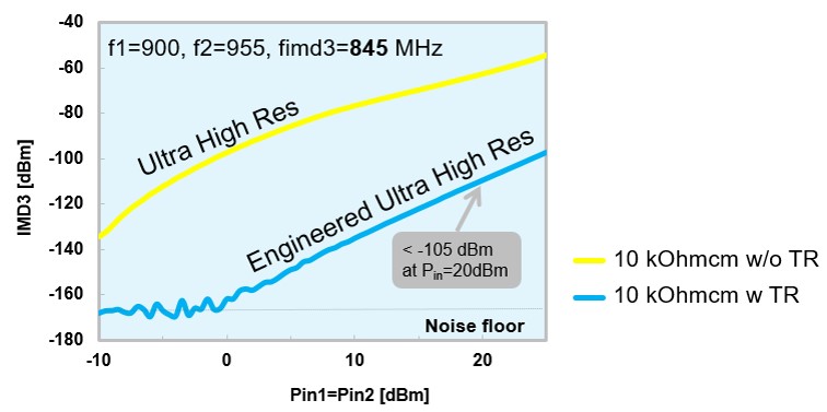
- Engineered Ultra High Resistivity wafers with trap-rich layer enable RF filters to reach extremely low IMD3 levels of even < -105 dBm at 845 MHz, measured at input power of 20 dBm. Measured with 2mm length 50Ω CPWs by Incize.
Extremely low IMD 3 levels with Engineered Engineered Ultra High Resistivity wafers
- The engineered trap-rich layer can be tailored to match the specific customer process to maximize the gains in harmonic behavior and overall losses.
- No need for complex implants and their effects on supply chain. The engineered trap-rich layer is purely silicon-based providing a good match for the customers’ production lines as no foreign materials are involved.
Engineered Ultra High Resistivity wafer solutions
Okmetic Engineered Ultra High Resistivity wafers are optimized, A-MCz® silicon wafers with low Oi, > 10,000 Ohm-cm resistivity and highly efficient trap-rich layer. These extremely high resistivities are enabled by Okmetic’s trademark Advanced Magnetic Czochralski (A-MCz®) crystal growth method. The Engineered Ultra High Resistivity wafer selection includes 200 mm SSP and DSP silicon wafers doped with Boron. Thicknesses range from 550 to > 1,150 µm. Crystal orientation <100> is available in volumes. Wafers in orientation <111> are ready for sampling. These wafers include UF-RFSi® (Ultra Flat High Resistivity wafer with trap-rich layer) and wafers for GaN-on-Si applications in RF (without trap-rich layer).
Engineered Ultra High Resistivity wafer specifications
| Growth method | A-MCz® |
| Diameter | 200 mm |
| Crystal orientation | <100> in volumes, <111> for sampling |
| P type dopants | Boron |
| Resistivity | >10,000 Ohm-cm |
| Oxygen | Typically ≤5 ppma or ≤10 ppma (ASTM F121-83). Can be optimized to Customer process. |
| SSP (etched backside) wafer thickness | 550 to 1,150 µm* *Other thicknesses possible with certain limitations |
| DSP (polished backside) wafer thickness | 550 to 1,150 µm* *Other thicknesses possible with certain limitations |
| Trap-rich layer | Purely silicon-based, no foreign materials |
Engineered Ultra High Resistivity wafer variations for specialized needs
Ultra High Resistivity wafer without trap-rich layer
Ultra High Resistivity wafer with low Oi, > 10,000 Ohm-cm resistivity, but without trap-rich layer. In this version the device maker can make the passivation / implantation by themselves.
Engineered Ultra High Resistivity wafer with Ultra Flat geometries
This wafer combines the ultra high resistivity of > 10,000 Ohm-cm to ultra flat geometries of UF-RFSi® wafer. This wafer has very low TTV (below 700nm) and non-circular symmetry variation. At the moment this wafer type is available for sampling.
Ultra High Resistivity RF GaN wafers for GaN-on-Si applications
This is the ultra high resistivity version of RF GaN wafers for GaN-on-Si applications. The wafer combines > 10,000 Ohm-cm to optimized Oi level and other wafer parameters decreasing wafer bow and warpage. At the moment this wafer type needs special review before sampling.
Ultra High Resistivity BSOI wafers
This is the ultra high resistivity version of BSOI wafers. The wafer combines > 10,000 Ohm-cm and optimized Oi to the layered structure of the SOI wafers. At the moment this wafer type is available for sampling.
See all 150-200 mm silicon wafers