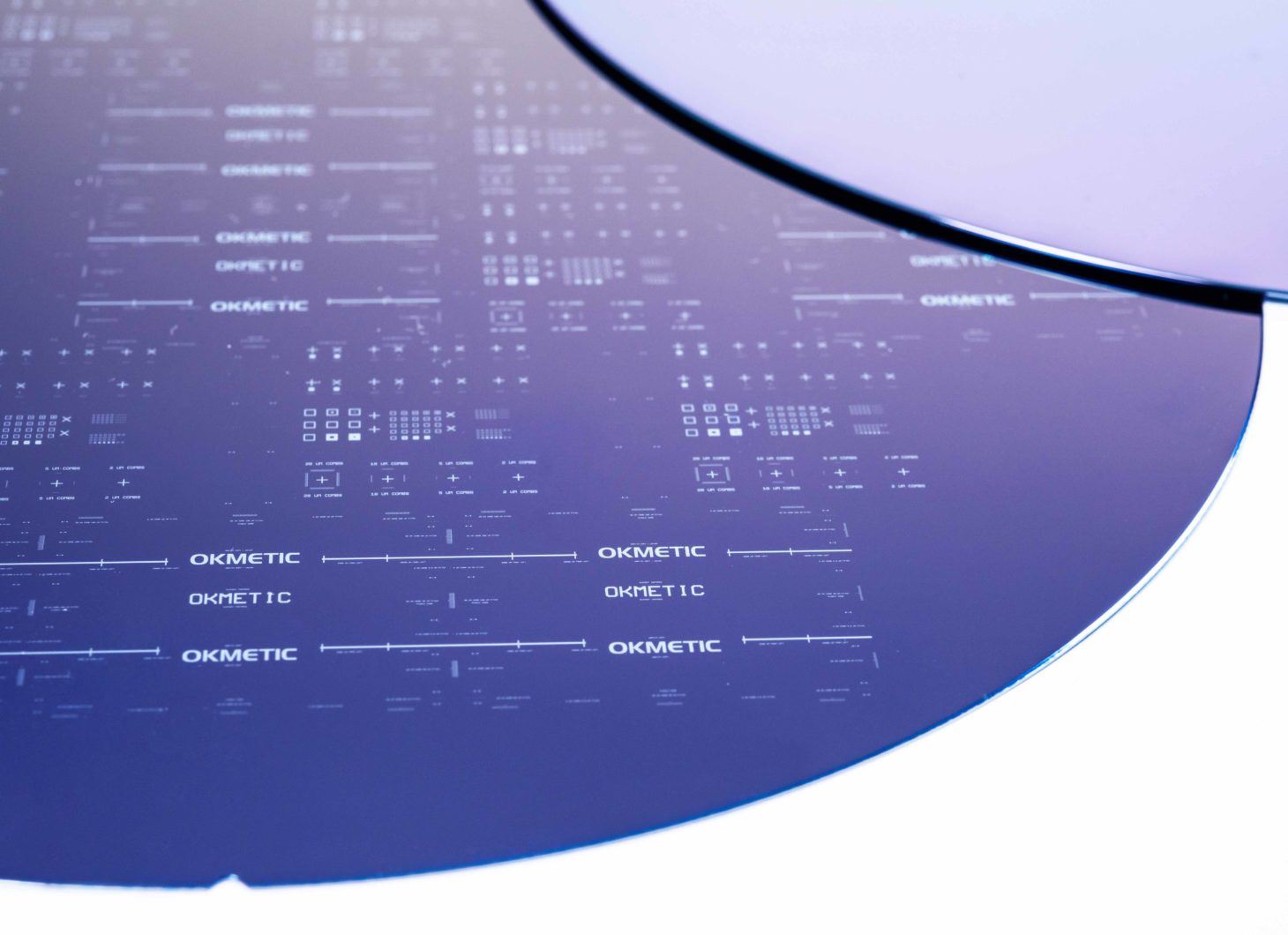
20 years of Okmetic SOI wafers – Bonded SOI wafers enable more ambitious device designs cost-effectively
Okmetic was among the first silicon suppliers to introduce bonded Silicon On Insulator technology and SOI wafers to the MEMS industry, and now the company has been volume producing SOI wafers for 20 years already. MEMS and sensor applications continue to be the main usage area even though SOI wafers are used more and more in power and RF applications as well.
Double-digit growth is forecast for the SOI market for the next five years with automotive and consumer electronics as well as healthcare applications being the main growth drivers. Growth is also fueled by the miniaturization of semiconductor devices as well as better device performance and lower total cost of ownership compared to devices using bulk silicon wafers as a platform.
Produced with 20 years’ of expertise and customized to match customer device and process needs seamlessly, Okmetic’s comprehensive line of SOI wafers provide an optimal platform for variety of applications:
- BSOI wafers – Bonded SOI (including BSOI variations 0.3 SOI)
- C-SOI® wafers – Cavity SOI
- E-SOI® wafers – Enhanced SOI, with tight thickness uniformity independent of the device layer thickness
- High Resistivity BSOI wafers are part of our RFSi® wafer family
Bonded SOI wafers’ layered structure is highly beneficial and widely used in applications such as advanced pressure sensors, inertial sensors, microfluidic components, MOEMS, flow sensors, actuators, silicon microphones, silicon photonics, ultrasonic transducers, high voltage applications such as gate drivers (IGBT/Power MOSFET), smart power/high voltage BCDs, lateral HV devices and also RF applications.
Bonding enables much thicker device layer and true freedom of design
Okmetic SOI wafers are manufactured by bonding two silicon wafers together and leaving an insulating buried oxide layer between them. Thanks to bonding process, the device layer of the SOI wafer can be made much thicker than with competing SOI technologies, which gives much more freedom to device design and enables true innovation.
The thicker device layer combined with high thickness uniformity enables a new level of device precision and performance. The Bonded SOI wafer device layer can range from 1 μm to over 200 μm with standard thickness tolerance being ±0.5 µm and even ±0.1 µm with Enhanced SOI (independent of the device layer thickness). E-SOI® enables advanced MEMS solutions such as high-performance low-loss silicon photonics, high-precision inertial sensors, and advanced ultrasonic transducers.
When considering the benefits of SOI wafers, one mustn’t forget the buried oxide layer, which is an excellent electric insulator and also forms an effective etch-stop in device manufacturing. The buried oxide can also be used as a sacrificial layer when manufacturing more complex devices such as released MEMS structures.
Okmetic SOI wafers enable additional design freedom, maximum device performance, cost-effectiveness and ease of manufacturing.
Cavity SOI streamlines MEMS manufacturing process
Okmetic has been producing C-SOI® wafers, meaning bonded SOI wafers with built-in sealed cavities since 2005. C-SOI® represents the most advanced silicon wafer technology and can be considered as a partially built sensor or electronic component rather than just a wafer.
The cavities built on the handle wafer or on the buried oxide are used to simplify and streamline device manufacturing and to enable processing of more complex and developed structures than would be possible with standard BSOI wafers. The cavities can also be used for integrations of IC and MEMS further increasing the usage possibilities.
Okmetic’s ability to produce C-SOI® wafers with extremely thin and thick membranes, well-defined horizontal dimensions and flexibility to adjust the gap between released structure and the substrate enable manufacturing of more advanced device designs. Cavity SOI wafers also enable the optimization of efficiency and electrical properties through minimization of parasitic capacitances. In addition, process optimization advantages can be gained through integrated backside packaging and hermetic sealing.
Cost-effectiveness through smaller die size
SOI wafers’ layered structure offers extremely cost-effective solution over bulk silicon micromachining and this is why more and more device manufacturers are turning for advanced wafer solutions.
As an example, when manufacturing a pressure sensor on 400 µm thick wafer the cost per chip can be reduced with standard bonded SOI wafer by 33% compared to bulk silicon wafers. This is because BSOI allows smaller die sizes and more chips per wafer thus reducing the wafer, patterning, etching and bonding costs. With C-SOI® wafers the reduction is even more: 50% compared to bulk silicon wafers and 25% compared to standard BSOI wafers.
Optimized performance through customization and high-quality processing
Okmetic’s SOI wafers are manufactured entirely in-house to ensure the highest quality SOI wafers. Thanks to the doubling of SOI capacity during 2019-2021 Okmetic has secured enough capacity for growing customer needs.
Along with high quality and state-of-the-art silicon technology customization is one of the key factors behind Okmetic SOI wafers’ success. The crystal and wafer parameters can be flexibly adjusted to create highly customized solutions tailored for customer’s product and process needs.


