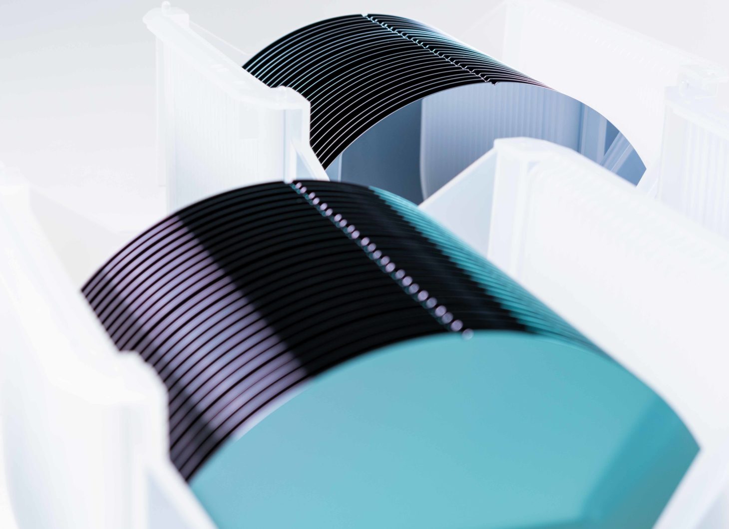
GaN on SOI substrates exhibit low stress and high crystalline quality
Okmetic has collaborated with the Finnish Aalto University for many years and provided tailored silicon wafers for different kinds of research purposes. The most recent collaboration concerns a study made by two of Aalto University’s researchers, Jori Lemettinen and Sami Suihkonen. They researched the MOVPE growth of Gallium Nitride (GaN) on 6 inch Silicon-On-Insulator (SOI) substrates and the effect of the substrate parameters on layer quality and strain. The results they obtained are very interesting and highly promising.
Lemettinen and Suihkonen’s research is very current as there has been increased attention within the field on the use of GaN on silicon for power electronics devices, such as rectifier diodes and high electron mobility transistors in particular. The reason for this attention is that GaN on silicon offers readily available substrates that are compatible with current CMOS fabs up to 8- inch in size. Silicon also exhibits high thermal conductivity, with clear benefits for power devices.
However, when using standard silicon substrates, the achievable material quality is limited by the lattice and thermal expansion mismatches. This is why it would seem that GaN on silicon is better suited for lower voltage power electronics (600-1200 V range) whereas GaN on silicon carbide (SiC) would be used for applications that require more performance.
A promising platform for power electronics applications
The starting point for Lemettinen’s and Suihkonen’s research was the fact that the use of SOI substrate had been suggested as having the ability to alleviate the detrimental effects of lattice and thermal mismatches and to absorb some of the stresses generated during epitaxy. Other studies had also demonstrated that the SOI substrate’s insulating buried oxide layer improves the breakdown characteristics of power electronics devices, enabling the useof GaN on silicon power electronics at higher operating voltage ranges. Hence, Lemettinen and Suihkonen wanted to research the effect of different substrate parameters on layer quality and strain more thoroughly.
In Lemettinen’s and Suihkonen’s research GaN layers were grown on 6 inch standard silicon substrate and SOI substrates with 1 µm and 2 µm buried oxide thicknesses. GaN layers were grown by using the standard step graded AlGaN and AlN low pressure metal-organic vapor phase epitaxy (MOVPE). The standard deviation of thickness was 1.25% and 1.36% for a nominally 2 µm thick epitaxial stack grown on standard silicon and SOI wafer, respectively.
GaN layers grown on SOI substrates exhibited lower stress and higher crystalline quality according to x-ray diffraction than the layers grown on standard silicon substrates.
Furthermore, growth on SOI substrate allows the use of a thinner AlGaN buffer compared to a standard silicon substrate while also maintaining the crystalline quality. A synchrotron radiation x-ray topography analysis confirmed that the stress relief mechanism of GaN on SOI epitaxy is the formation of a dislocation network on the device’s silicon layer. The buried oxide layer significantly improves the vertical leakage characteristics as the onset of breakdown is delayed by approximately 400 V. These results confirm that GaN on SOI is a promising platform for power electronics applications.
As a result, it can be said that box layer significantly improves the the vertical leakage characteristics. Currently, Okmetic is conducting research cooperation with several partners in order to further development on the high resistivity of GaN. The results will be published in the second quarter.


