Okmetic launches Terrace Free SOI capability
Vantaa, Finland – March 22, 2023 – Okmetic, the leading supplier of advanced silicon wafers for the manufacture of MEMS, sensor, RF and power devices, today announced the release of Terrace Free SOI capability for its 200 mm Bonded Silicon-On-Insulator BSOI and E-SOI® wafers.
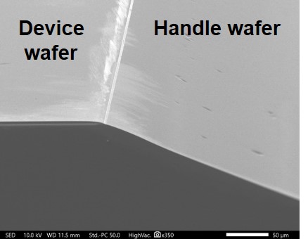
The Terrace Free SOI wafers provide device manufacturers with maximized usable area and enable more chips per wafer to be produced. The standard SOI terrace (non-SOI area) is ≤ 2 mm so the Terrace Free SOI wafers provide a prominent, ca. 4%, increase in the active area. Also, the Fixed Quality Area (FQA) increases by ca. 3% as a result of edge exclusion area decrease from 4.5 mm to 3.0 mm.
The Terrace Free SOI wafers’ edge is beveled into optimal shape to enhance compatibility with subsequent device processing. Terrace Free SOI wafers can e.g. facilitate wafer clamping and handling as well as epitaxial growth and lithography process including resist coating.
“Okmetic’s motivation to develop Terrace Free SOI wafers was to meet the customer and industry needs. To be able to manufacture a fully Terrace Free SOI wafer, Okmetic needed to develop a new kind of optimized version of the established SOI process. Okmetic is very pleased of being able to collaborate with several pilot customers in the development phase. These customers gave valuable feedback on the Terrace Free SOI wafer prototypes, which has enabled more rapid development phase and made the subsequent production ramp-up successful. Upon the launch of this Terrace Free SOI capability, Okmetic is now ready to provide samples and start volume deliveries for a wider audience”, says Atte Haapalinna, Chief Technology Officer at Okmetic.
Availability
Terrace Free SOI capability is available for 200 mm Bonded Silicon-On-Insulator BSOI and E-SOI® wafers, which provide an optimal platform for the manufacture of MEMS, RF and power devices. For sales information, sample shipments and custom quotes, please contact your regional sales representative.
About Okmetic
Okmetic, founded in 1985, is the leading supplier of advanced, high value-added silicon wafers for the manufacture of MEMS, sensor, RF and power devices. Okmetic has the most extensive 150 to 200 mm wafer portfolio in the market, comprising comprehensive lines of Silicon-On-Insulator (SOI) wafers and High Resistivity RFSi® wafers as well as Patterned wafers, SSP and DSP wafers, TSV wafers, Wafers for Power devices and Wafers for GaN-on-Si applications.
Okmetic’s headquarters is located in Finland, where the majority of the company’s silicon wafers is manufactured. Worldwide sales organization and technical support ensure quick local service, rapid prototyping and highly optimized wafer solutions. Okmetic’s operations rely on quality and environmental systems in line with the ISO 9001:2015, ISO 14001:2015, and IATF 16949:2016 standards. In 2021, Okmetic net sales were 128 MEUR, but the company is to more than double its capacity and business along with the new 400 MEUR fab investment announced in May 2022. To learn more, visit www.okmetic.com.
Media Contact
CTO Atte Haapalinna, Okmetic
Tel. +358 9 502 80 474, atte.haapalinna@okmetic.com
Marketing Manager Marika Mäntymaa, Okmetic
Tel. +358 40 069 7882, marika.mantymaa@okmetic.com


