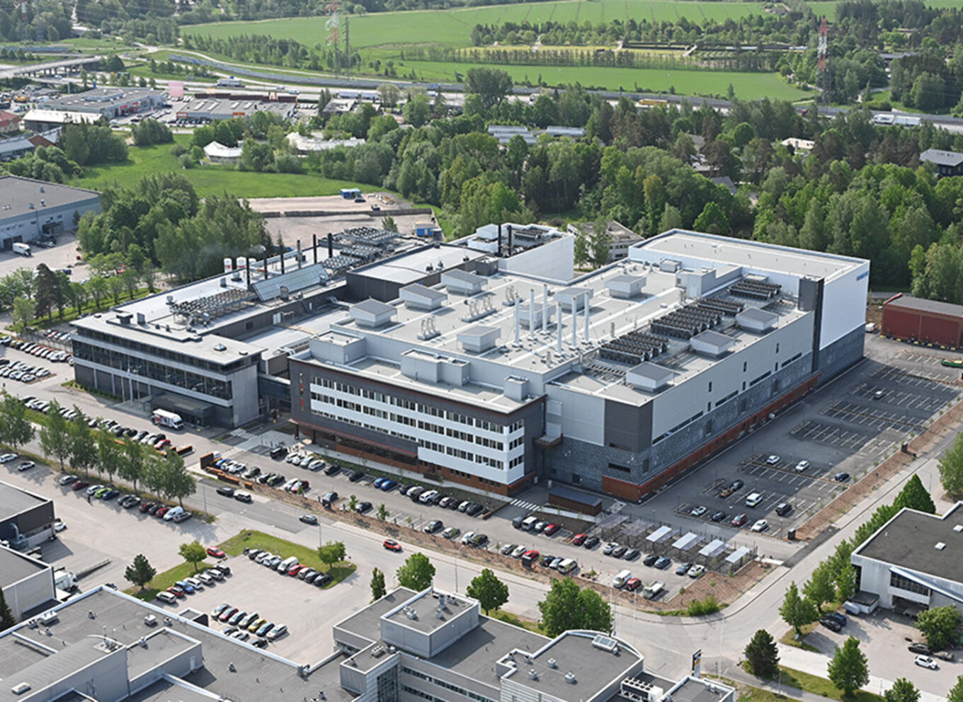
Okmetic’s form of company is now Oy
News+2/7/2017
Okmetic’s changed information and company bylaws has been updated into Finnish Trade Register on January 31, 2017. The new form of company is now Okmetic Oy.
Okmetic’s changed information and company bylaws has been updated into Finnish Trade Register on January 31, 2017. The new form of company is now Okmetic Oy.