We focus heavily on research and development work
We have developed our unique technological expertise by ourselves and have always been ready to innovate and take our business operations to the next level. We also collaborate closely with the leading research institutes in the industry and customers that develop high-technology solutions.
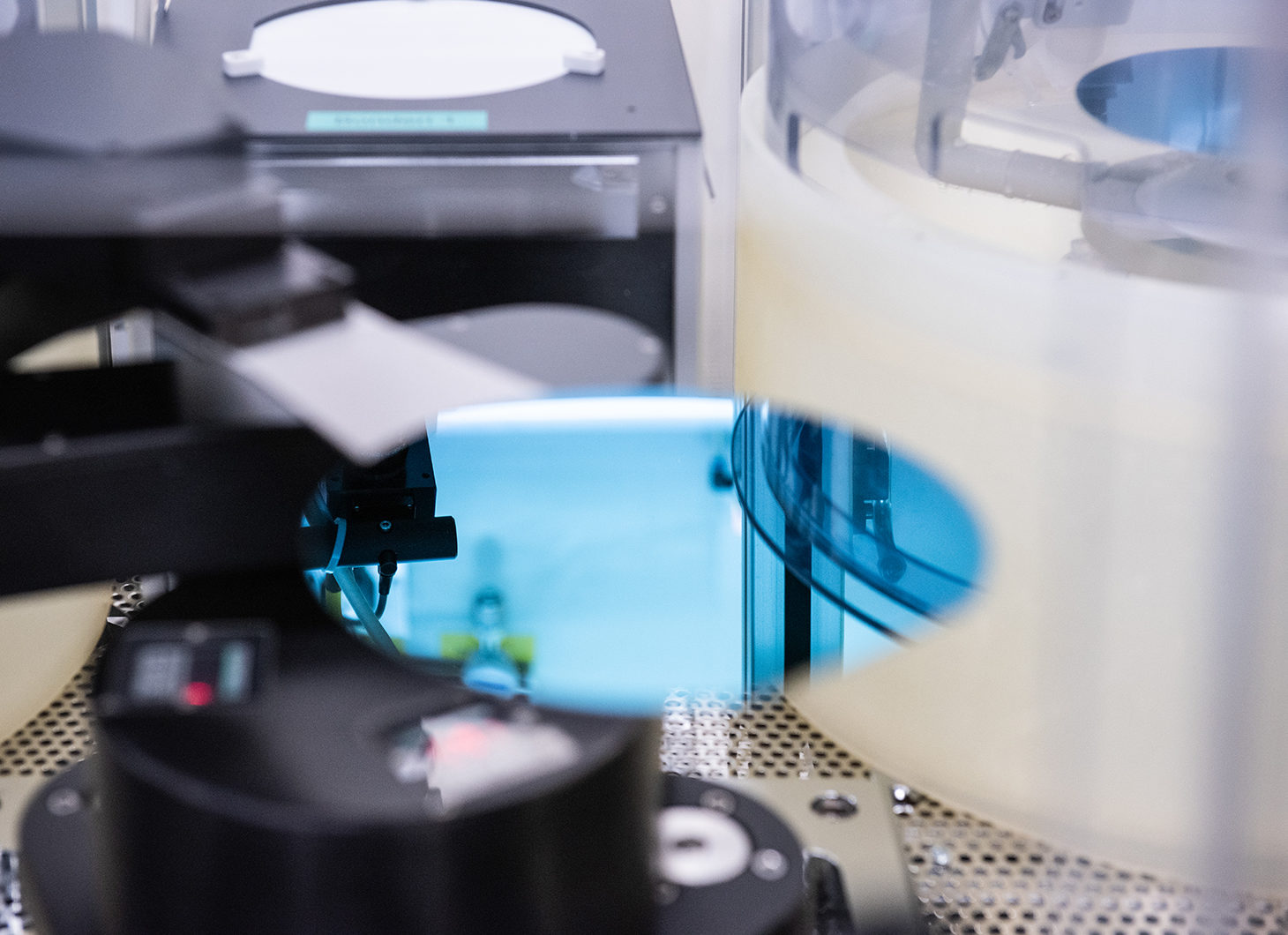
The role of research and development work in our company has been pivotal since the beginning. Ever since we started the production of advanced silicon wafers in 1985 as pioneers, our corporate culture has been honed to support research and development. Even to this day, our values are based on customer orientation, sustainable growth, respecting and valuing others and continuous improvement of operations.
Throughout our history, we have participated in multiple national and EU-funded R&D collaboration projects together with Technical Research Centre of Finland, Aalto University, and several European research institutes and semiconductor manufacturers. In recent years, we have participated in projects that continue to create conditions for the changes in the telecommunications infrastructure (5G) or develop autonomous cars for the upcoming generations (ADAS).
We are an active operator in the EU projects of the semiconductor industry developing groundbreaking microelectromechanical systems. We are also part of the wide-scale MEMS cluster in Finland.
The focus of Okmetic’s research and development work is in the crystal growing technology, production processes of specialty wafers, and the development of wafer patterning and DRIE etching processes. Due to the efforts in these areas, we are able to deliver tailor-made SOI wafers, high resistivity RFSi® wafers, power wafers and 200 mm wafers in large volumes based on our customer needs.
We often collaborate with our customers starting from the beginning of the product development process all the way to the end of the life cycle. Sales and technical customer support help us identify the optimal solutions, and our agile organization in the production of fast prototypes.
The goal of product development is to work ideas and prototypes into products suitable for volume production, whereas the role of process development lies in ensuring the performance of production processes and cost-efficiency even in the future.
We are involved in many R&D projects

Beetles project
Okmetic is partaking in Beetles project which is a Finnish project consortium coordinated by VTT and funded by Business Finland. In this project Okmetic is developing its low-loss high resistivity silicon substrates to meet the constantly evolving requirements of advanced RF filters and other RF devices. The project demonstrates that substrate-induced losses in RF devices are effectively mitigated by optimized silicon wafer material

RF Sampo
RF SAMPO, the leading ecosystem project of the Nokia Veturi program, is an industrial joint venture funded by Business Finland, Okmetic, nine other companies, and three research organizations. The goal of the RF SAMPO project is to strengthen Finland’s competitiveness in radio frequency technologies, to speed up the development of RF and antenna technologies and to accelerate the transition from 5G to 6G.
The European Chips Skills Academy
Europe faces a significant shortage of microelectronics professionals, with over 320 000 new employees needed and 100 000 set to retire in the next seven years. The European Chips Skills Academy (ECSA) aims to address this gap by enhancing skills development and industry collaboration. Okmetic will share best practices to support Finland’s semiconductor industry. Supported by the EU, ECSA aligns with policies like the EU Chips Act to strengthen the microelectronics sector.