White paper: “Enabling next-gen power and RF GaN devices with optimized silicon and SOI substrates”
Gallium Nitride (GaN) is a leading material for power and RF devices due to its superior properties. However, growing high-quality GaN layers on silicon presents mechanical and thermal challenges. This whitepaper explores how optimized silicon and bonded SOI substrates support reliable GaN epitaxy by managing stress, reducing defects, and improving wafer stability. It also highlights the benefits of GaN-on-SOI for enabling integrated, compact device designs.
Holistically optimized Si substrates for GAN growth: Engineered to overcome growth challenges improve GAN filmquality and boost power and RF device performance
GaN-on-SOI for advanced devices: Combining GaN’s performance with bonded SOI’s isolation to enable monolithic integration in efficient, compact power and RF solutions
Proven at scale: Nearly half a million wafers delivered to date for high-yield GaN growth
Introduction
Gallium Nitride (GaN) is rapidly gaining prominence in the semiconductor industry due to its exceptional material properties, enabling outstanding performance in high-power electronics, RF (radio frequency) applications, LEDs and optoelectronics. GaN’s wide bandgap, high breakdown voltage, and high electron mobility allow devices to operate effectively at higher voltages, temperatures, and frequencies compared to traditional silicon-based technologies (Fig 1). These attributes make GaN an ideal choice for power and RF applications where efficiency, reliability, and performance are crucial.
However, growing high-quality GaN layers on silicon substrates presents several challenges. The significant lattice mismatch and thermal expansion coefficient difference between GaN and silicon can lead to high dislocation densities, wafer bowing, and even crack formation during high-temperature epitaxy. These mechanical and thermal stresses must be carefully managed to ensure device reliability and manufacturing yield.
While GaN-on-Silicon and GaN-on-SOI offer cost and scalability advantages, addressing the intrinsic challenges of lattice and thermal mismatch requires a combination of advanced buffer layer engineering and optimized substrate design.
This whitepaper explores the role of optimized silicon wafers and bonded Silicon-On-Insulator (SOI) substrates in supporting GaN growth, focusing on their advantages for power and RF devices. While GaN-on-Silicon and GaN-on-SOI offer cost and scalability advantages, addressing the intrinsic challenges of lattice and thermal mismatch requires a combination of advanced buffer layer engineering and optimized substrate design. By tailoring key parameters in both Si and SOI substrates such as wafer thickness, interstitial oxygen concentration, edge profile, and resistivity, it is possible to mitigate stress, suppress defect formation, and improve mechanical stability during GaN epitaxy. In addition to these benefits, GaN-on-SOI offers the added advantage of monolithic integration, which enables multiple functions to be built on a single chip and further simplifying overall device architecture. These combined advantages make both Si and bonded SOI substrates well-suited for GaN applications in power conversion, LED devices, 5G, and other high-frequency systems.
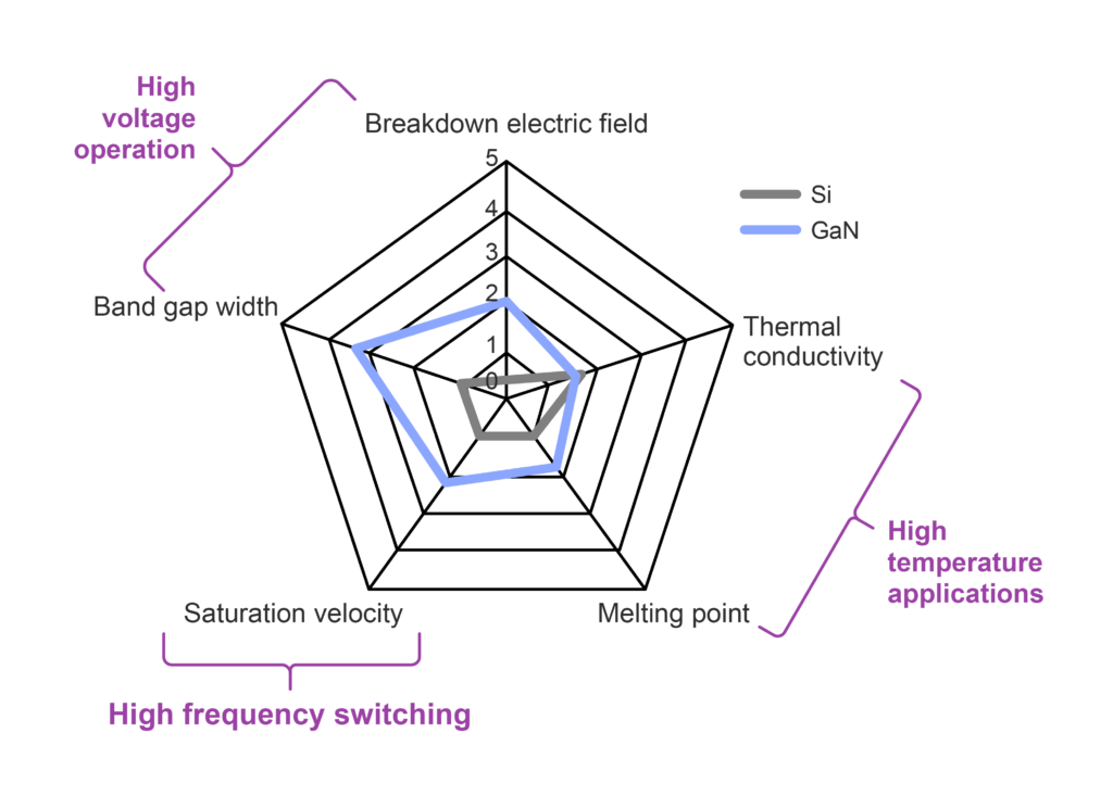
Figure.1 Comparison of GaN with Si.
GaN growth and substrate selection
GaN growth has become increasingly critical for high-performance power and RF applications. Epitaxial methods, such as Metal-Organic Chemical Vapor Deposition (MOCVD), are commonly used to grow GaN on various substrates, including silicon (Si), bonded Silicon-On-Insulator (SOI), silicon carbide (SiC), and sapphire. As illustrated in Figure 2, each substrate offers distinct advantages and challenges in terms of GaN growth, affecting factors like cost, thermal management, and lattice matching.
Although SiC and sapphire are much more suitable for GaN growth in terms of thermal and lattice mismatch, they are expensive, limited in wafer size, and they cannot easily be integrated into standard Si-based processes.
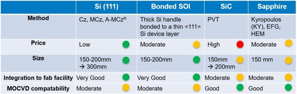
Figure 2 Different substrates for GaN epitaxial growth.
Silicon is cost-efficient and scalable choice
Silicon wafers are significantly more affordable and widely available compared to SiC wafers, making them an economical choice for manufacturers. In addition to lower material costs, Si wafers support large-scale production thanks to their CMOS compatibility and availability in larger sizes (up to 300 mm), which increases number of dies per wafer. The mature silicon supply chain and existing manufacturing infrastructure further reduce costs by eliminating the need for specialized equipment, making Si an ideal platform for GaN on Si technologies. Moreover, GaN-on-Si manufacturing is generally more environmentally friendly compared to GaN-on-SiC [Vanhouche], as SiC production requires higher energy consumption and involves more resource-intensive processes.
In addition to lower material costs, Si wafers support large-scale production thanks to their CMOS compatibility and availability in larger sizes (up to 300 mm), which increases number of dies per wafer.
Among Si-based options, bonded Silicon-On-Insulator (SOI) substrates have emerged as a promising alternative for GaN growth, offering enhanced crystalline quality and fewer cracks due to improved stress management during epitaxy [Lemettinen]. The advantages of SOI, including its potential for monolithic integration of power and RF components, make it an attractive path for next-generation GaN device platforms.
How substrate optimization helps overcome GaN-on-Si challenges
Thermal expansion and lattice mismatch between GaN and Si create significant mechanical stresses during GaN growth and cooling (Fig.3). These stresses can lead to wafer bowing, warping, cracking, and high dislocation densities, which impact device performance and yield negatively. Addressing these mechanical challenges is critical for achieving high-quality GaN epitaxy on silicon substrates.
While epitaxy engineering, particularly buffer layer design, is critical for managing stress and reducing dislocations, one important enabler of successful GaN-on-Si growth lies in the use of a high-quality, optimized silicon substrate.
While epitaxy engineering, particularly buffer layer design with materials such as AlN or AlGaN, is critical for managing stress and reducing dislocations (Fig. 4), one important enabler of successful GaN-on-Si growth lies in the use of a high-quality, optimized silicon substrate. An optimized silicon substrate provides the mechanical stability and surface quality required to support advanced epitaxial structures and enhance overall GaN film performance.
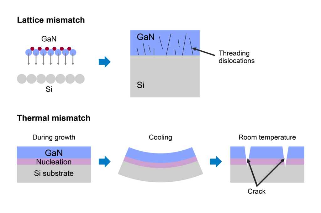
Figure 3. Lattice and thermal mismatch for GaN-on-Si. Upper picture: GaN has a different (larger) lattice constant compared to Si, which introduces strain during nucleation. This can lead to defects like threading dislocations as the system tries to relieve the stress. Lower picture: During cooling from high temperature, Si shrinks more than GaN, causing bowing/warping and crack formation in the GaN film if the Si substrate is not optimized for GaN growth.
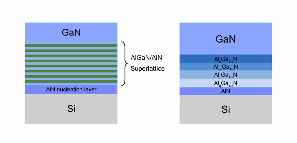
Figure 4. A schematic representation of two commonly used buffer layer designs: superlattice buffer (left) and step graded buffer (right) are used for GaN-on-Si growth on optimized silicon substrates. Alongside buffer engineering, the quality and optimization of the silicon substrate plays a crucial role in managing stress and defects, providing the mechanical stability needed for successful GaN epitaxy. The superlattice buffer consists of repeated AlGaN/AlN layers to gradually address lattice and thermal mismatch, while the step graded buffer varies aluminum content layer-by-layer to relax strain and reduce wafer bowing.
Optimized Si substrates for high-quality GaN epitaxy
A holistic approach to substrate engineering is key to successful GaN-on-Si growth. Several substrate parameters can be fine-tuned to support high-quality epitaxy and reduce stress-related defects:
- <111> orientation with tight surface orientation tolerance helps manage strain, reduce lattice mismatch effects and improve yield
- Thicker wafers minimize in-situ curvature, ensuring uniform epitaxy
- Controlled impurities such as Oi prevents slip, enhancing mechanical strength
- Engineered edges optimize gas flow and thermal distribution for consistent processing
- Optimized resistivity for RF or Power device needs
Orientation and thickness
Silicon, particularly with <111> orientation and tight surface orientation, is commonly selected for GaN growth as it offers better lattice compatibility, helping to reduce strain and enhance crystal quality during epitaxy.
However, due to the significant mismatch in lattice constants and thermal expansion coefficients between Si and GaN, thicker silicon wafers are often needed to manage the mechanical and thermal stresses induced during high-temperature processing. In-situ wafer curvature measurements are used to monitor real-time changes in wafer bow, providing insights into stress evolution and mechanical stability during growth.
As shown in Fig. 5, the thicker 1,000 µm wafer exhibits a more stable and smoother curvature evolution compared to the thinner 725 µm wafer, which shows greater fluctuations and larger curvature variations. This demonstrates that increasing wafer thickness enhances mechanical stability and reduces curvature sensitivity during GaN epitaxy. A more stable wafer bow or warp contributes to improved layer uniformity and helps mitigate potential yield issues such as misalignment, localized stress, or defect formation.
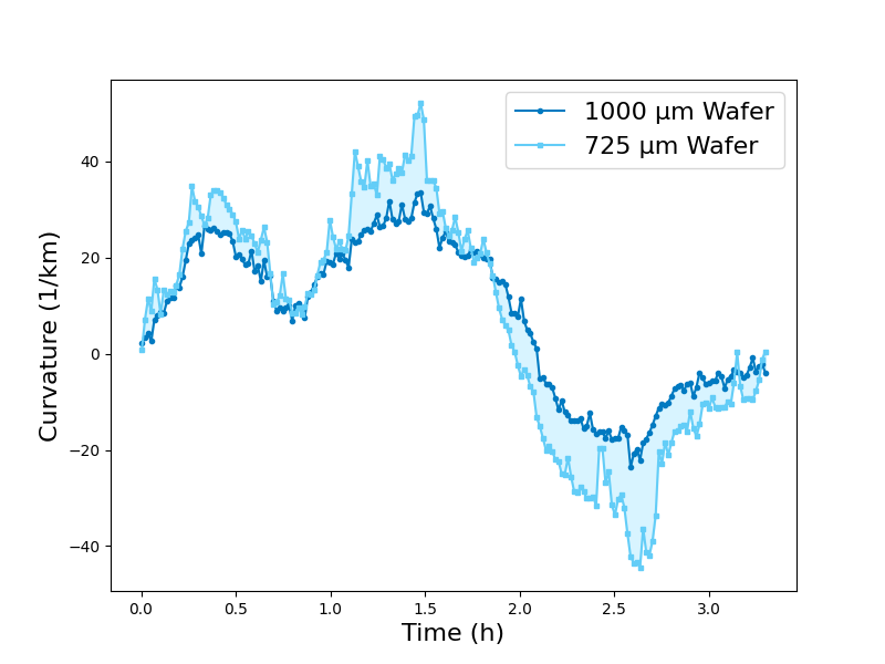
Figure 5. In-situ wafer curvature over time during epitaxy. The thicker 1,000 µm wafer exhibits a more stable and smoother curvature evolution compared to the thinner 725 µm wafer, which shows greater fluctuations and larger curvature variations. A more stable wafer bow or warp contributes to improved layer uniformity and helps mitigate potential yield issues such as misalignment, localized stress, or defect formation.
Controlled oxygen
Furthermore, precise control of interstitial oxygen (Oi) levels in the silicon substrate is crucial for enhancing mechanical strength and improving wafer stability. A well-managed Oi concentration increases the wafer’s resistance to slip formation, helping to minimize warpage and ensuring greater durability during the high-temperature conditions of GaN epitaxy. Slip lines are dislocation networks that form due to plastic deformation under thermal stress, and their presence can indicate mechanical damage within the wafer.
A well-managed Oi concentration increases the wafer’s resistance to slip formation, helping to minimize warpage and ensuring greater durability during the high-temperature conditions of GaN epitaxy.
Oxygen precipitates, small clusters of oxygen atoms formed during thermal processing, can play a helpful role. When sufficiently small, they can pin dislocations [Zeng, Sueoka] and enhance the material’s strength, making it more resistant to deformation. These precipitates typically form during high-temperature treatments, where excess oxygen atoms in the silicon lattice migrate and cluster together. While higher interstitial oxygen levels tend to promote more precipitate formation and improve mechanical performance, their growth must be carefully controlled to avoid introducing unwanted defects.
As shown in Fig. 6 from the X-ray diffraction imaging (XRDI) analysis, wafers with optimized Oi levels (Fig. 6 b) exhibit significantly fewer slip lines compared to non-optimized wafers (Fig. 6 a), highlighting the importance of Oi control for maintaining wafer integrity. Fewer slip lines lead to enhanced device performance and greater mechanical stability, ensuring higher reliability in GaN-based applications.
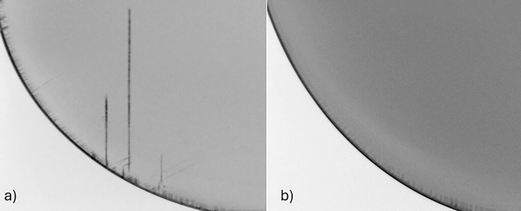
Figure 6. XRDi shows Oi optimized wafer (b) has fewer slip lines compared to (a) non-optimized wafer. Fewer slip lines in GaN growth indicate lower stress and improved material quality.
Edge engineering
Engineered wafer edges play an essential role in optimizing GaN epitaxy by promoting uniform gas flow and thermal distribution across the wafer surface. Proper edge shaping reduces local temperature gradients and suppresses boundary-related anomalies that can lead to non-uniform film thickness or defects. This enhances the overall consistency of the growth process, improving epitaxial layer uniformity, surface morphology, and ultimately device yield. Edge engineering is particularly critical in large-diameter wafers where edge effects are more pronounced and can impact both process stability and material quality.
Edge engineering enhances the overall consistency of the growth process, improving epitaxial layer uniformity, surface morphology, and ultimately device yield.
Resistivity
The resistivity of the silicon wafer plays a critical role in GaN-on-Si epitaxy, influencing both the growth process and the final device performance. Okmetic’s Advanced Magnetic Czochralski (A-MCz®) crystal growth process offers high-quality silicon substrates with carefully tailored resistivity levels to meet the specific requirements of both RF and power applications.
Okmetic’s Advanced Magnetic Czochralski (A-MCz®) crystal growth process offers high-quality silicon substrates with carefully tailored resistivity levels to meet the specific requirements of both RF and power applications.
For power electronic applications, low-resistivity silicon wafers (typically <0.02 Ohm-cm) are commonly used. In power devices, the epitaxial stack is generally thicker, requiring a more mechanically robust substrate to maintain structural integrity during processing and operation.
In contrast, for RF applications, high resistivity silicon wafers (typically >1,000 Ohm-cm) are preferred to minimize unwanted interactions between the RF signal and the silicon substrate. This reduces RF signal losses and enhances linearity and signal integrity, which are critical factors for high-frequency, high-linearity devices such as RF switches and power amplifiers.
Selecting the appropriate wafer resistivity is therefore key to optimizing both the mechanical and electrical performance of GaN-on-Si devices for different target markets.
GaN-on-SOI is an emerging technology
GaN-on-SOI (Gallium Nitride on Silicon-On-Insulator) is an emerging technology gaining significant traction in semiconductor applications, particularly in power electronics and RF devices. It combines the high-performance characteristics of GaN with the electrical isolation and mechanical benefits of SOI, offering substantial improvements in device efficiency and overall performance. GaN-on-SOI technology addresses key challenges, such as electrical isolation and reduced parasitic effects, making it an ideal platform for next-generation devices in both power and RF applications.
GaN-on-SOI is an emerging technology combining the high-performance characteristics of GaN with the electrical isolation and mechanical benefits of SOI, offering substantial improvements in device efficiency and overall performance.
A key advantage of GaN-on-SOI is its ability to enable monolithic integration, which simplifies device architecture by combining multiple functions on a single substrate. This integration enhances reliability, and allows for more compact designs. As the demand for higher efficiency and miniaturization in advanced electronic systems grows, GaN-on-SOI is well-positioned to drive the next generation of semiconductor innovation. The buried oxide (BOX) layer in bonded SOI significantly reduces parasitic capacitance, leakage, and crosstalk, leading to faster switching speeds, lower conduction losses, and superior isolation that are critical for high-voltage power conversion.
Okmetic (bonded) GaN SOI Substrate wafers are specifically designed to optimize GaN performance, offering the ideal platform for developing advanced GaN devices in both power and RF applications. Our substrates are engineered to meet the requirements of these applications, while providing superior electrical isolation, low defectivity, strong thermal performance, and mechanical robustness. Just like our GaN Silicon Substrate wafers, all parameters of our GaN SOI Substrate wafers can be customized to meet the specific requirements of your application, including:
- Device layer thickness, orientation, resistivity, Oi levels
- BOX (buried oxide) thickness
- Handle wafer thickness, orientation, resistivity, Oi levels
Whether you’re working on high-voltage power conversion or next-gen RF systems, our wafers are tailored to deliver optimal performance for your specific needs.
GaN-on-SOI enabling monolithic integration
Monolithic integration of GaN devices on advanced substrates such as bonded SOI wafers offers significant benefits across power, RF, and LED applications by simplifying system design, enhancing performance, and reducing parasitic losses.
Monolithic integration of GaN devices on advanced substrates such as bonded SOI wafers offers significant benefits across power, RF, and LED applications by simplifying system design, enhancing performance, and reducing parasitic losses.
Most GaN power systems today are composed of multiple discrete chips. Devices such as GaN HEMTs are typically fabricated separately and then assembled onto a printed circuit board. While this modular approach is common, it introduces complexity, increases cost, and can limit overall system efficiency.
A more effective alternative is monolithic integration, where multiple GaN power devices are fabricated together on a single chip. One topology that benefits significantly from this approach is the half-bridge converter, which comprises both a low-side and a high-side switch. These switches operate at different voltage potentials, requiring effective electrical isolation. Monolithic integration can address this through advanced substrate and isolation strategies, including the buried oxide (BOX) layer found in bonded SOI wafers. This not only simplifies packaging and reduces parasitic losses but also enhances performance in compact power systems.
Okmetic’s Bonded SOI Power GaN substrates
Okmetic’s bonded SOI Power GaN Substrate wafers offer an excellent platform for all-GaN ICs, as they minimize cross-talk and back-gating effects [Li], providing superior electrical isolation and enhanced device performance. This performance is achieved by using a SOI substrate for GaN epitaxial growth combined with a trench isolation method (Fig.7), which fully isolates the high electron mobility transistor (HEMT) and its respective Si device layer. The backgating effect can be fully eliminated by connecting the source terminals to their respective Si <111> device layer.
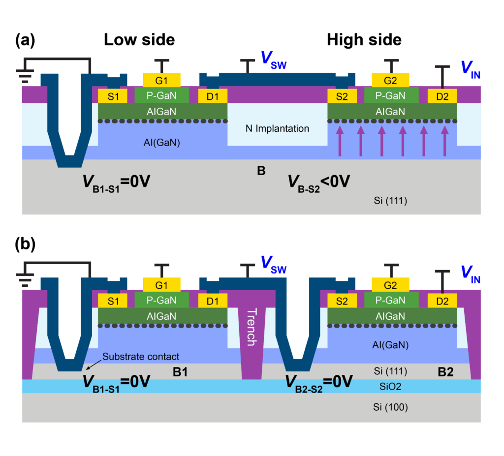
Figure 7. Schematic cross-section of monolithically integrated half-bridge with e-mode low side and high side devices fabricated on 200 mm (a) GaN-on-Si, and (b) GaN-on-SOI with trench isolation. From [Li].
As shown in Fig. 8 transfer characteristics undergo very little change when the SOI substrate of the neighboring device is biased between -200 V and 200 V. In contrast, when this occurs on a silicon substrate, transfer characteristics shift, indicating performance degradation in these devices. This integration approach reduces parasitic inductances, decreases die size, eliminates back-gating effects, and ultimately enhances power efficiency.

Figure 8. Transfer characteristics of a HEMT at 150°C (a) with a common silicon substrate biased from -200 V to 200 V (GaN-on-silicon) and (b) while simultaneously biasing the neighboring silicon <111> HEMT layer at different voltages (GaN-on-SOI), showing very little effect. From [Li].
Okmetic-IMEC GaN-on-SOI Power device collaboration
Recent study (2024) by Interuniversity Microelectronics Centre (IMEC) examined Okmetic’s GaN-optimized and non-optimized SOI wafers, comparing their effects on GaN growth, wafer bowing, and stability. IMEC successfully grew a 4.4 µm GaN-epi-stack on Okmetic bonded SOI wafers (Fig. 9). The results highlight the critical role of substrate-induced mechanical stability in enabling high-quality GaN epitaxy under thermal and mechanical stress conditions.
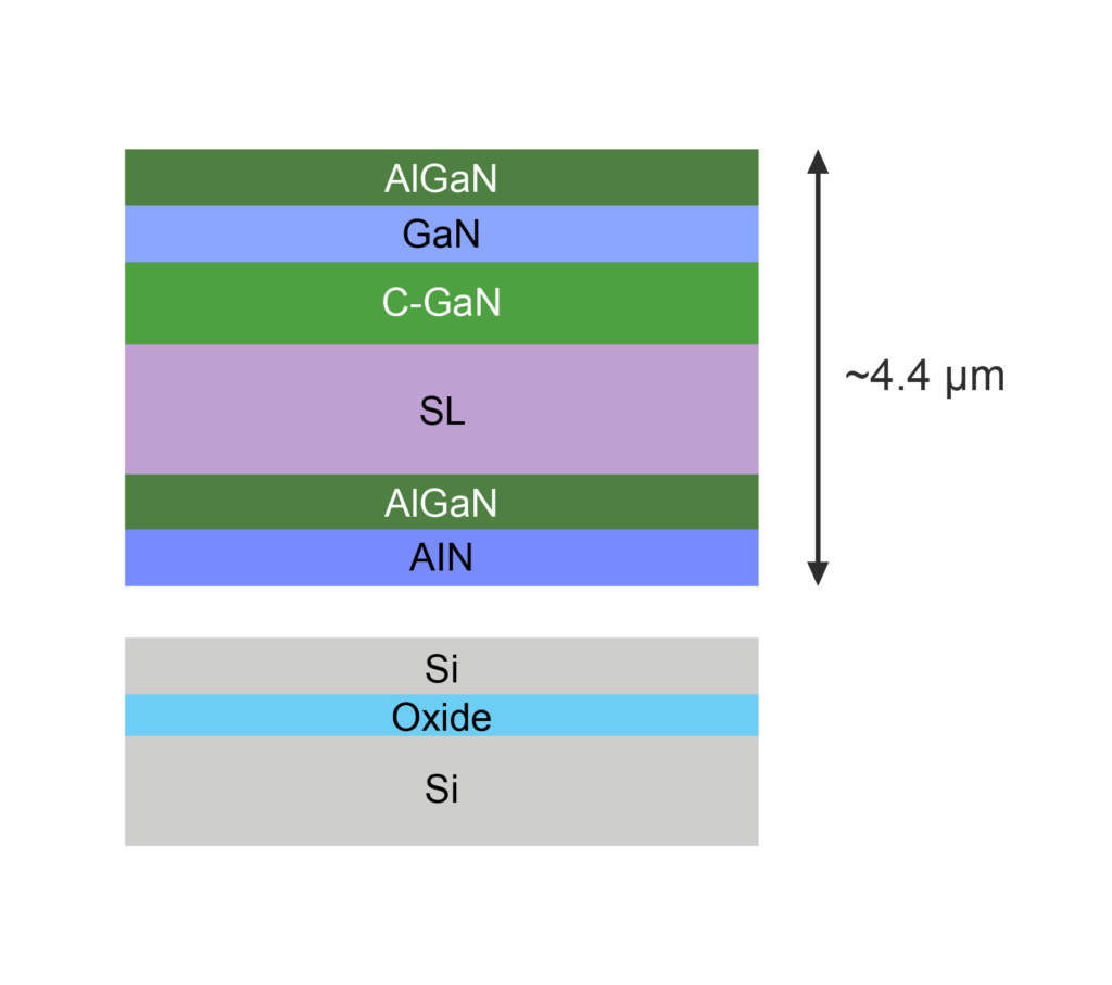
Figure 9. Employed qualification epi stack by IMEC grown on Okmetic GaN SOI Substrate wafer.
Both GaN-optimized and non-optimized SOI wafers had identical specifications for the device and buried oxide layers, as well as for handle layer thickness. Both wafers also utilized a <111> crystal orientation, known for enhancing wafer durability. The key distinction between the two types of wafers lies in the GaN-optimized SOI wafers, which feature higher doping and oxygen interstitial concentrations in the handle layer. This optimization substantially improves wafer robustness and stability during the high-temperature GaN growth process, providing an ideal platform for GaN epitaxy without compromising structural integrity.
GaN-optimized SOI wafers’ robustness and stability during the high-temperature GaN growth process provides an ideal platform for GaN epitaxy without compromising structural integrity.
Okmetic-IMEC GaN-on-SOI electrical testing
Electrical testing confirms the wafers’ suitability for high-performance GaN devices, with low leakage currents, high buffer breakdown voltages (750V reverse, 850V forward), and minimal trapped charge effects, as evidenced by dispersion measurements (Fig. 10a and b). Additionally, the uniform AlGaN cap layer with minimal thickness variation (Fig. 10c) ensures stable 2DEG properties and reliable threshold voltage in GaN HEMTs, supporting long-term reliability and performance in advanced power applications.
Electrical testing confirms the wafers’ suitability for high-performance GaN devices with low leakage currents, high buffer breakdown voltages, and minimal trapped charge effects.
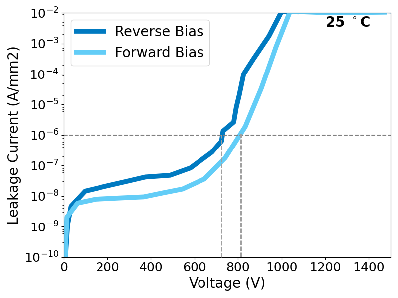
Figure 10 a. Okmetic Power GaN SOI Substrate wafers, used as a platform for GaN epitaxy, achieved a very low leakage current of 10-6 A/mm2 at ~750V in reverse bias (25°C) and 850V in forward bias during IMEC’s buffer layer breakdown voltage measurements conducted on small-area samples (0.01 mm2).
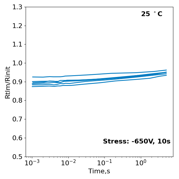
Figure 10 b. IMEC’s buffer dispersion measurements on Okmetic Power GaN SOI Substrate wafers, used as a platform for GaN epitaxy, indicate minimal trapped charge effects. The minimal curve widening observed highlights excellent device performance.
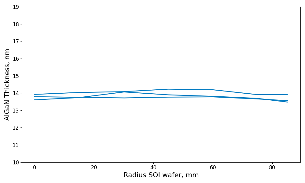
Figure 10 c. X-ray reflectometry measurements of thickness variation of the AlGaN cap layer along the wafer radius. AlGaN cap layer is very important for the device performance, so variation in 1 nm is crucial.
Applicability of GaN-on-SOI to RF devices
Okmetic’s bonded SOI GaN substrate wafers offer significant advantages for RF GaN device applications. Key benefits include monolithic integration capability, low parasitic capacitance, reduced substrate losses, high electrical isolation, and crucially, compatibility with standard CMOS integration processes—features that are highly valuable in high-frequency RF systems. Studies [Tham], [Jiang] have shown that SOI substrates can reduce vertical leakage and enhance the epitaxial layer quality of GaN devices. The substrate architecture can be tailored by adjusting the BOX thickness and selecting device and handle wafer parameters to meet the demanding performance criteria of RF components. These factors enable monolithic integration, which supports greater circuit compactness and improved overall RF system performance when using Okmetic’s bonded SOI RF GaN substrate wafers.
Okmetic’s bonded SOI GaN Substrate wafers enable monolithic integration with low parasitic capacitance and high electrical isolation, delivering enhanced performance and compactness for high-frequency RF GaN devices.
Conclusion
GaN-on-Si technology is becoming increasingly important for both RF and power applications, driven by the need for higher efficiency, improved thermal management, and cost-effective scaling. Between 2020 and 2024, Okmetic has successfully delivered approximately 500,000 substrates, demonstrating strong market acceptance and proven reliability of its solutions.
Silicon substrates offer stable performance for GaN devices along with unmatched cost-efficiency, scalability, and environmental benefits, while bonded SOI substrates open up new possibilities for integration and enhanced device performance. Achieving high-quality and reliable GaN-on-Si and GaN-on-SOI devices requires a comprehensive approach that addresses multiple critical wafer properties. Optimizing silicon orientation, wafer thickness, interstitial oxygen concentration, edge and resistivity is essential for managing mechanical strain, minimizing wafer bow and slip formation, and enhancing device performance. Each of these parameters plays a distinct role. Therefore, a holistic optimization of wafer characteristics is key to enabling robust, high-yield GaN growth processes tailored to the specific demands of RF and power electronic applications.
Okmetic’s continued development of GaN-optimized silicon and SOI substrates, validated by collaborations such as the recent IMEC study, highlights the company’s commitment to enabling next-generation GaN technologies. With customizable wafer parameters tailored to specific device needs, Okmetic substrates provide a robust and reliable platform for advancing power conversion and RF communication.
List of references used in this white paper can be found in the downloadable pdf version.