
White paper “Advancing from 4G LTE to 5G and 6G: Engineered RFSi® silicon wafers for high-performance RF devices”
As wireless technologies move from 4G LTE to 5G and 6G, RF filters and devices face increasing demands for higher bandwidth, better linearity, and improved isolation. This whitepaper explains how engineered high resistivity silicon wafers with a trap-rich layer help address challenges like parasitic surface conductivity and strict surface uniformity requirements. These wafers enhance the performance and manufacturing yield of acoustic filters (TF-SAW, BAW) and integrated passive devices used in key high-frequency bands.

Unlocking performance: Engineered High Resistivity silicon wafers with trap-rich layers reduce insertion loss and signal distortion in advanced RF devices.
Future-ready RF design: 5G/6G, carrier aggregation, and wideband filters are supported with ultra-flat, low-loss substrates.
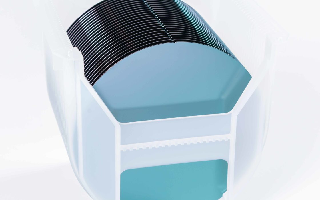
Proven at scale: Over 3 million RFSi® wafers delivered for high-yield, high-efficiency RF front-end manufacturing.
Introduction
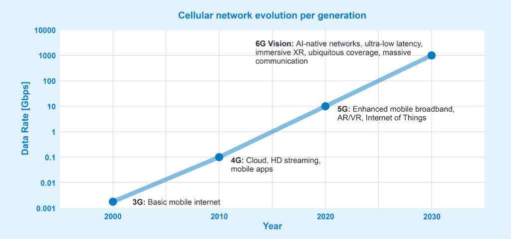
The evolution from 4G LTE to 5G and emerging 6G technologies has driven an unprecedented demand for higher data transmission rates, greater bandwidths, and more complex RF architectures, increasing the need for advanced RF filters and devices that meet stringent requirement for loss, linearity, and isolation. High-power user equipment (HPUE) and wider bandwidths, such as those in N77 and N79 bands, challenge conventional technologies. Acoustic filters (TF-SAW, BAW) and integrated passive devices (IPD) face increasingly ambitious specifications to support advancements such as carrier aggregation and new power standards, driving the demand for high-performance solutions like high resistivity silicon wafers.
As system complexity and performance expectations grow, traditional high-resistivity silicon wafers are being tested by new challenges in suppressing unwanted coupling and maintaining signal interference. One key issue is parasitic surface conductivity (PSC), which arises at the Si-SiO₂ interface and degrades effective resistivity, linearity, and isolation. Additionally, the use of thin piezoelectric films in TF-SAW increases sensitivity to the substrate’s topography and thickness variation, imposing stricter uniformity requirements that impact both performance and yield.
This whitepaper explores how Engineered High Resistivity silicon wafers with a trap-rich layer can overcome these challenges and enhance RF filter and device performance. It highlights the mechanisms behind PSC and its suppression, the critical roles of both the trap-rich layer and high nominal resistivity in achieving low harmonic and intermodulation distortion, and the importance of precise surface topography and thickness control for effective piezoelectric layer bonding.
By addressing both electrical and geometrical challenges, these substrates enable RF designers to meet the increasingly demanding specifications of next-generation wireless technologies.
RF filters and devices rely on Engineered High Resistivity wafers
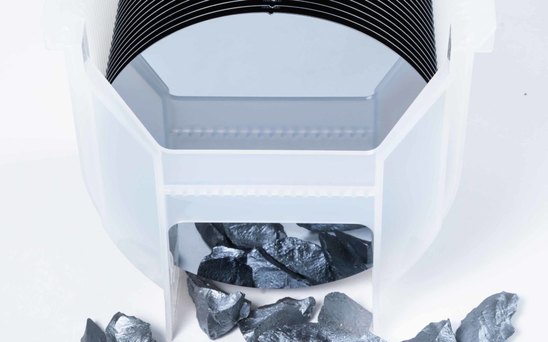
RF filters and devices typically rely on Engineered silicon wafers specified with high nominal resistivities and a trap-rich layer to minimize unwanted interactions between the RF signal and the silicon substrate. Achieving resistivity levels often exceeding 1,000 Ohm-cm or even 10, 000 Ohm-cm requires extremely low nominal doping in the crystal ingot. Okmetic’s Advanced Magnetic Czochralski (A-MCz®) technology is specially designed to achieve these high resistivity levels.
Okmetic’s A-MCz® technology enables ultra high resistivity levels exceeding 10,000 Ohm-cm, making its engineered RFSi® wafers ideal for RF filters and devices that demand minimal signal interference and superior uniformity.
Okmetic offers a range of engineered RFSi® silicon wafers optimized to meet the stringent requirements of RF filters and devices, ensuring minimal unwanted interactions between the RF signal and the silicon substrate:
- Engineered High Resistivity wafers
- Engineered Ultra High Resistivity wafers
- UF-RFSi® wafers that have high thickness uniformity and precise surface geometries
Parasitic surface conductivity and its suppression with a trap-rich layer
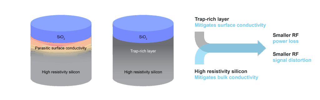
Figure 2. Together with high resistivity silicon wafer, a trap rich layer eliminates parasitic surface conductivity and eliminates substrate-induced losses and nonlinearity.
High nominal resistivity alone is often insufficient to achieve the desired linearity due to an effect known as parasitic surface conductivity (PSC). In RF device manufacturing, a thin silicon dioxide (SiO₂) layer is commonly placed as an intermediate layer between the silicon substrate and subsequent piezoelectric or metal layer to improve device isolation and acoustic properties.
However, in SiO₂-Si interface as well as other insulator-semiconductor interfaces, there are fixed charges inherently present. These charges induce a highly conductive layer below the buried oxide. This causes unwanted coupling of the RF field to the conductive layer, causing signal distortion and nonlinearity, including harmonic and intermodulation distortion. It also has a detrimental impact on device quality factor, insertion loss and crosstalk of RF devices.
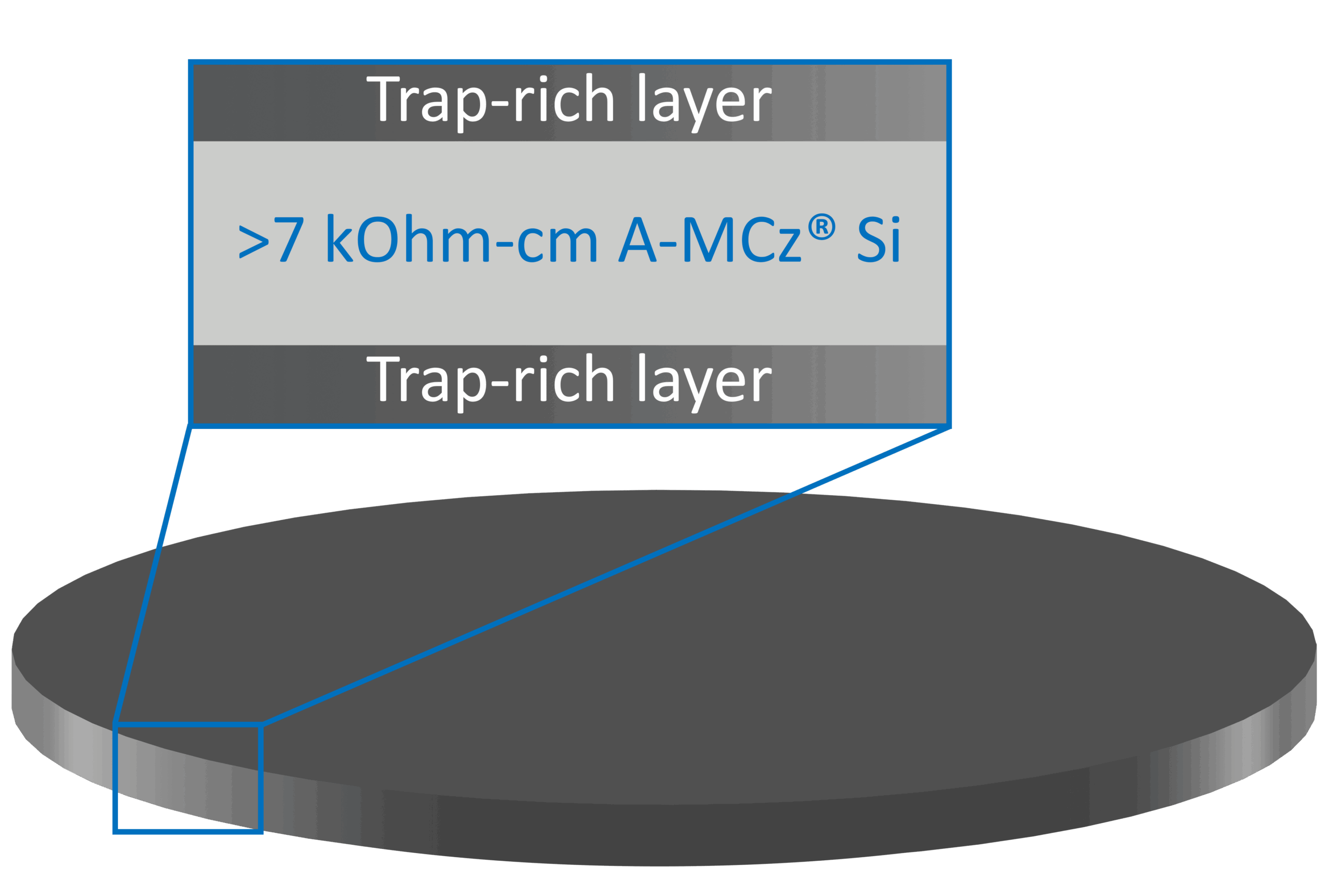
Parasitic surface conductivity at the SiO2-Si interface is mitigated in Okmetic’s Engineered High Resistivity and Engineered Ultra High Resistivity wafers, which include a trap-rich layer beneath the SiO2 layer applied by the device manufacturer.
Parasitic surface conductivity at the SiO₂-Si interface is mitigated in Okmetic’s Engineered High Resistivity and Engineered Ultra High Resistivity wafers, which include a trap-rich (TR) layer beneath the SiO₂ layer applied by the device manufacturer. A trap-rich layer, with its high density of dangling bonds, effectively “traps” or “freezes” mobile charge carriers, preventing them from contributing to conduction. The trap-rich layer manufactured by Okmetic is purely silicon-based, contains no foreign materials, and meets stringent surface quality and cleanliness requirements.
Trap-rich layer ensures high effective resistivity of the substrate for optimal RF performance
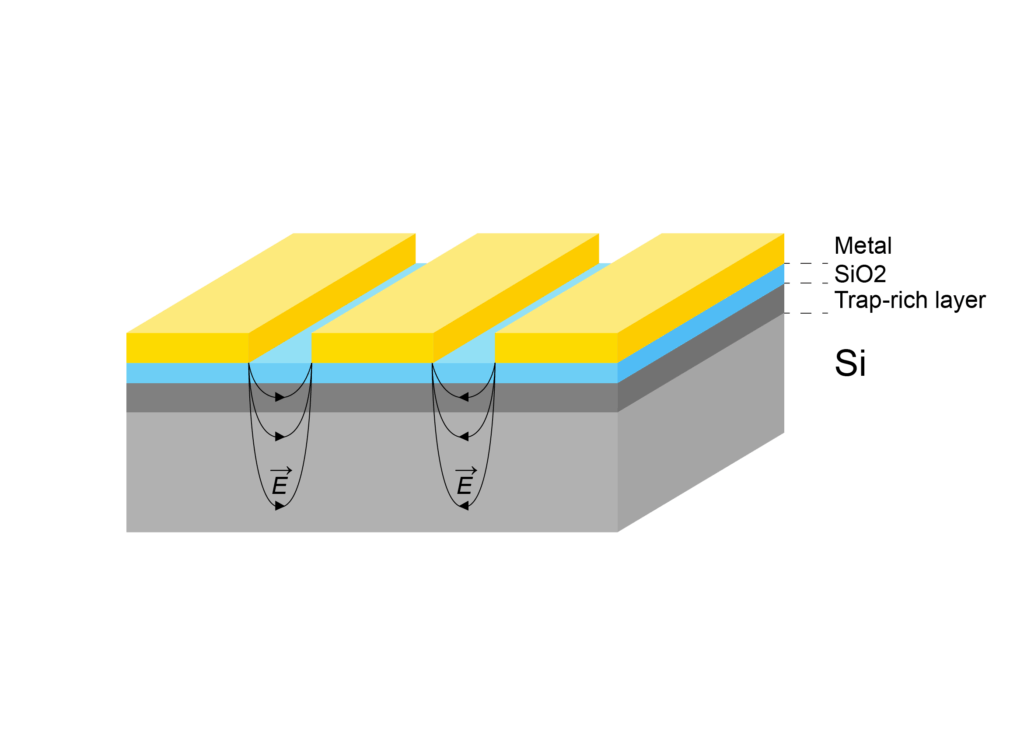
The performance of silicon wafers in RF devices can be significantly enhanced by the presence of a trap-rich layer. This layer is critical in maintaining high resistivity of the substrate, which minimizes unwanted conductivities that can affect the overall RF performance. In silicon wafers without this layer, the effective resistivity is typically around 100 Ohm-cm, as determined from S-parameter measurements on coplanar waveguide (CPW) test structures based on the RLCG model.
To evaluate the effect on loss and linearity, 2 mm-long CPW test structures with a characteristic impedance of 50 Ohms were employed, reflecting a common standard in RF substrate benchmarking. The fabrication of the test structures and the measurements, which are showcased in this and the following chapters, were conducted by Incize.
The presence of a trap-rich layer in high resistivity wafers ensures significantly higher effective resistivity, leading to lower signal losses, improved isolation, and enhanced overall RF performance.
In Fig. 3, we compare the signal attenuation and effective resistivity of high-resistivity wafers with and without a trap-rich layer. The top illustration shows the schematic layout and electric field penetration in the substrate. The presence of a trap-rich layer in high resistivity wafers ensures significantly higher effective resistivity, leading to lower signal losses, improved isolation, and enhanced overall RF performance.
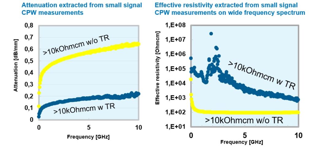
Figure 3. Attenuation and effective resistivity extracted from S-parameter measurements on CPW test structure. High resistivity wafers with a trap-rich layer show significantly lower RF losses due to suppressed parasitic surface conductivity that ensures high resistivity and signal integrity.
Suppression of second harmonic distortion
In the evolving landscape of 5G and 6G development, increasingly ambitious specifications for losses and linearity are required to support emerging technologies like carrier aggregation and new power standards. Among various forms of nonlinear distortion, second harmonic distortion is particularly critical due to its direct impact on RF signal integrity. This type of distortion is strongly influenced by the characteristics of the silicon wafer. The effect is clearly illustrated in the second harmonic measurement presented in Fig. 4, obtained using the same CPW test structures at a base frequency of 900 MHz across varying input power levels.
Parasitic surface conductivity significantly influences the second harmonic output power, with levels being 50 dB higher when no suppression method is applied. Incorporating a trap-rich layer into the silicon wafer effectively eliminates the parasitic surface conductivity, but the wafer’s resistivity also plays a critical role. Silicon wafers with resistivity exceeding 10,000 Ohm-cm offer up to 10 dB more suppression compared to 5,000 Ohm-cm silicon wafers, resulting in significantly improved RF performance and reduced harmonic distortion. This advantage becomes particularly evident at high power levels, where effective suppression is essential.
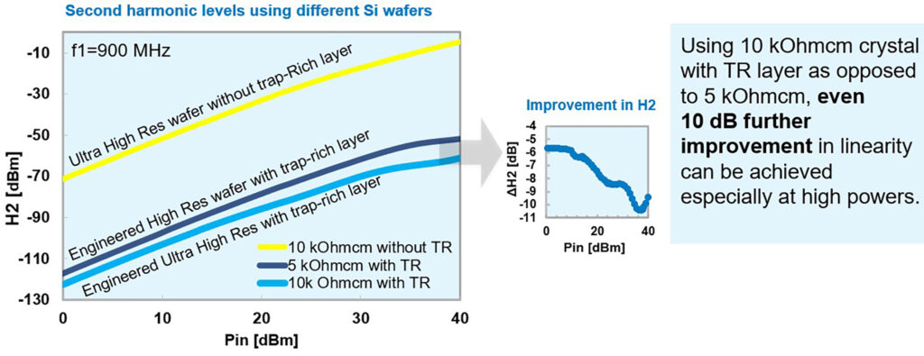
Figure 4. Engineered High Resistivity silicon wafers with a trap-rich layer enable suppression in second harmonic by tens of decibels. Additionally, Ultra High Resistivity further enhances linearity, reducing signal degradation.
Suppression of third harmonic and intermodulation distortion
Third harmonic (H3) distortion and intermodulation distortion (IMD) are critical factors affecting the performance of RF systems. H3 introduces unwanted spurious frequencies that interfere with the desired signal, while IMD occurs when multiple signals mix, leading to distortion that degrades system linearity, efficiency, and signal integrity. Suppressing these distortions is essential for maintaining high-quality RF device performance.
While H3 and IMD3 are typically more sensitive to losses in metals and interconnects than to losses in the silicon bulk, the results demonstrate that substrate engineering with a trap-rich layer can still significantly enhance linearity, yielding improvements of several tens of decibels in both H3 and IMD3 levels.
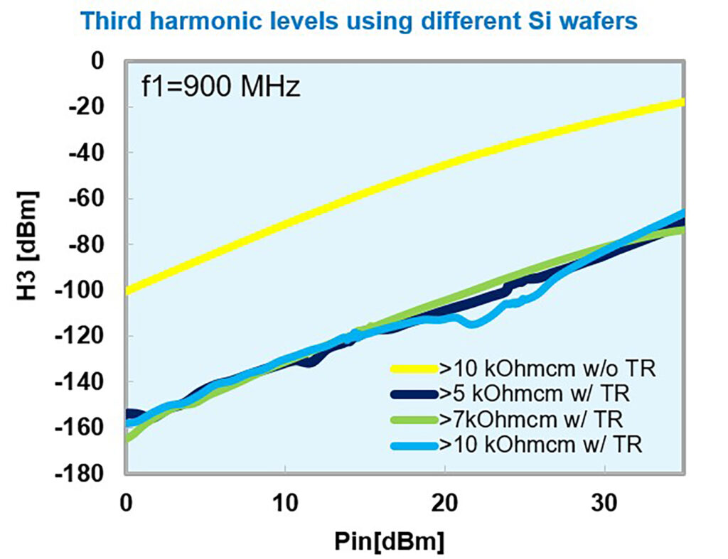
The incorporation of a trap-rich layer in the high resistivity silicon wafer significantly suppresses third harmonic (H3) and intermodulation distortion (IMD), as shown in Fig. 5. H3 was measured using 900 MHz input tone, and the third order intermodulation distortion (IMD3) was measured using input tones at 900 MHz and 955 MHz from the same CPW test devices.
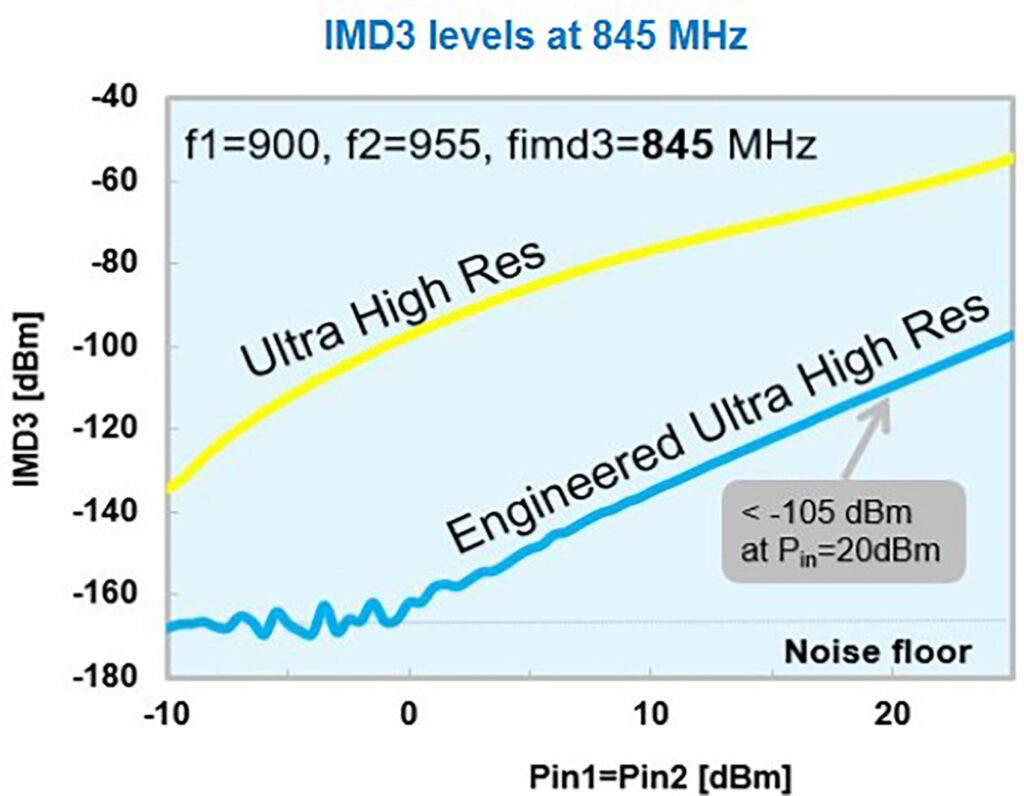
While H3 and IMD3 are typically more sensitive to losses in metals and interconnects than to losses in the silicon bulk, the results demonstrate that substrate engineering with a trap-rich layer can still significantly enhance linearity, yielding improvements of several tens of decibels in both H3 and IMD3 levels.
Figure 5. Third harmonic and intermodulation distortion measurements with CPW test structures showcase the improvements in linearity with advanced silicon wafers.
Improved layer thickness uniformity enhances TF-SAW filter yield
In thin-film surface acoustic wave devices (TF-SAWs), the thickness uniformity of the piezoelectric layer directly impacts device yield. A thin single crystalline LiTaO3 film is manufactured on top of the silicon wafer by bonding and thinning, and the thin LiTaO3 film is ion beam trimmed to reach better film thickness uniformity. The thin film inherits the silicon wafer’s geometrical properties, replicating both macroscopic thickness variations and microscopic surface features.
Developed especially for TF-SAW applications, Okmetic’s specialized UF-RFSi® wafer offers an optimal platform with ultra-flat topography, high resistivity, low insertion loss, and superior linearity.
Developed especially for TF-SAW applications, Okmetic’s specialized UF-RFSi® wafer offers an optimal platform with ultra-flat topography, high resistivity, low insertion loss, and superior linearity. With very low Total Thickness Variation (TTV) and minimal non-circular symmetry variation, it enables more efficient planarization of the device layer and reduces the need for trimming in bonding and grind-back processes.
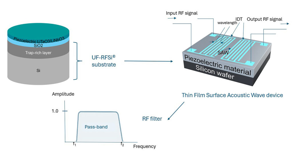
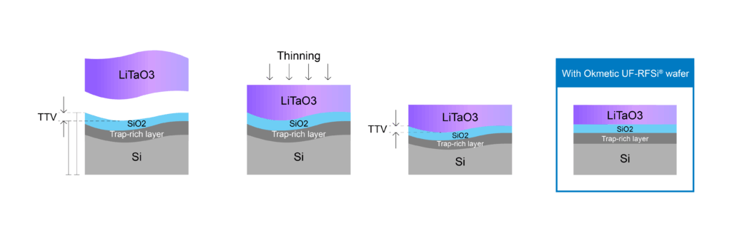
Figure 6. In TF-SAW manufacturing, silicon wafer total thickness variation is copied into the LiTaO₃ layer. Okmetic UF-RFSi® wafers offer ultra-flat topography with very low TTV, reducing non-uniformity, minimizing post-processing, and boosting filter yield and performance.
RFSi® wafer key features and benefits
Next-generation RF filters and front-end devices demand substrates with exceptional electrical performance and precise dimensional control. Okmetic’s Engineered High Resistivity, Engineered Ultra High Resistivity, and UF-RFSi® wafers are specifically designed to meet these needs. With resistivities up to 10,000 Ohm-cm and a highly efficient, purely silicon-based trap-rich layer, these wafers effectively suppress parasitic effects that degrade linearity and signal integrity.
Key benefits include minimal second harmonic and IMD3 distortion, near-zero substrate-induced losses, and very low total thickness variation (TTV) option, which ensures high yield and superior device performance in advanced RF applications.
Engineered Ultra High Resistivity wafers
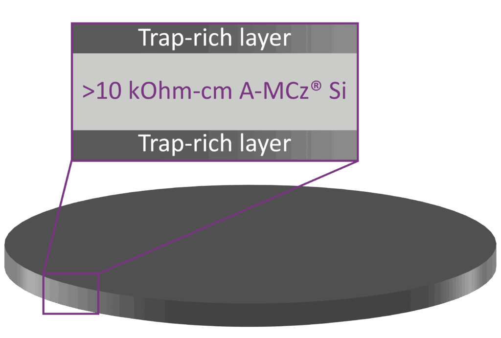
- Optimized A-MCz® silicon wafer with low Oi and >10 kOhm-cm resistivity
- Trap-rich layer and doping process taken to extremes
- Best technical performance: close to zero substrate induced losses and nonlinearities
- Available in 200 mm
- Premium solution for RF filters
Engineered High Resistivity wafers
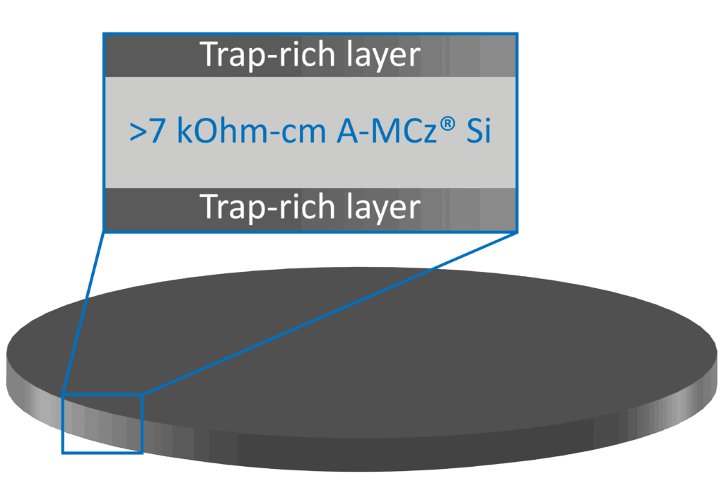
- Optimized A-MCz® silicon wafer with low Oi, up to >7 kOhm-cm resistivity and trap-rich layer
- Enabling superior RF performance and very low losses
- Available in 150- 200mm
- For RF filter and IPD devices
UF-RFSi® wafers
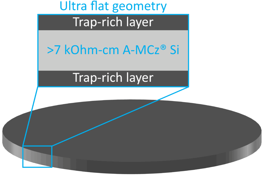
- Optimized A-MCz® silicon wafer with low Oi, up to >7 kOhm-cm resistivity and trap-rich layer
- Trap-rich layer and Ultra Flat geometries with very low TTV + non-circular symmetry variation
- Enabling superior RF performance and challenging active layer geometries
- Available in 150- 200mm
- Also available in Ultra High Resistivity version
- For TF-SAW devices
Conclusion
The transition to 5G and the development of 6G technologies place increasingly stringent demands on RF filter and device performance, particularly in terms of loss, linearity, and isolation. Okmetic’s Engineered High Resistivity wafers (RFSi®), including Ultra High Resistivity and UF-RFSi® variants, provide a proven foundation for meeting these challenges. By integrating a purely silicon-based trap-rich layer and achieving resistivities up to 10,000 Ohm-cm, these wafers effectively suppress parasitic surface conductivity, minimize harmonic and intermodulation distortion, and support high signal integrity even under high power operation.
With precise thickness uniformity and surface control, these wafers also meet the demanding yield and performance requirements of advanced filter technologies such as TF-SAW. Having delivered over 3 million RFSi® wafers globally, Okmetic continues to empower RF designers and manufacturers with reliable, high-performance substrates tailored for next generation wireless systems.


