E-SOI complements Okmetic’s SOI product family
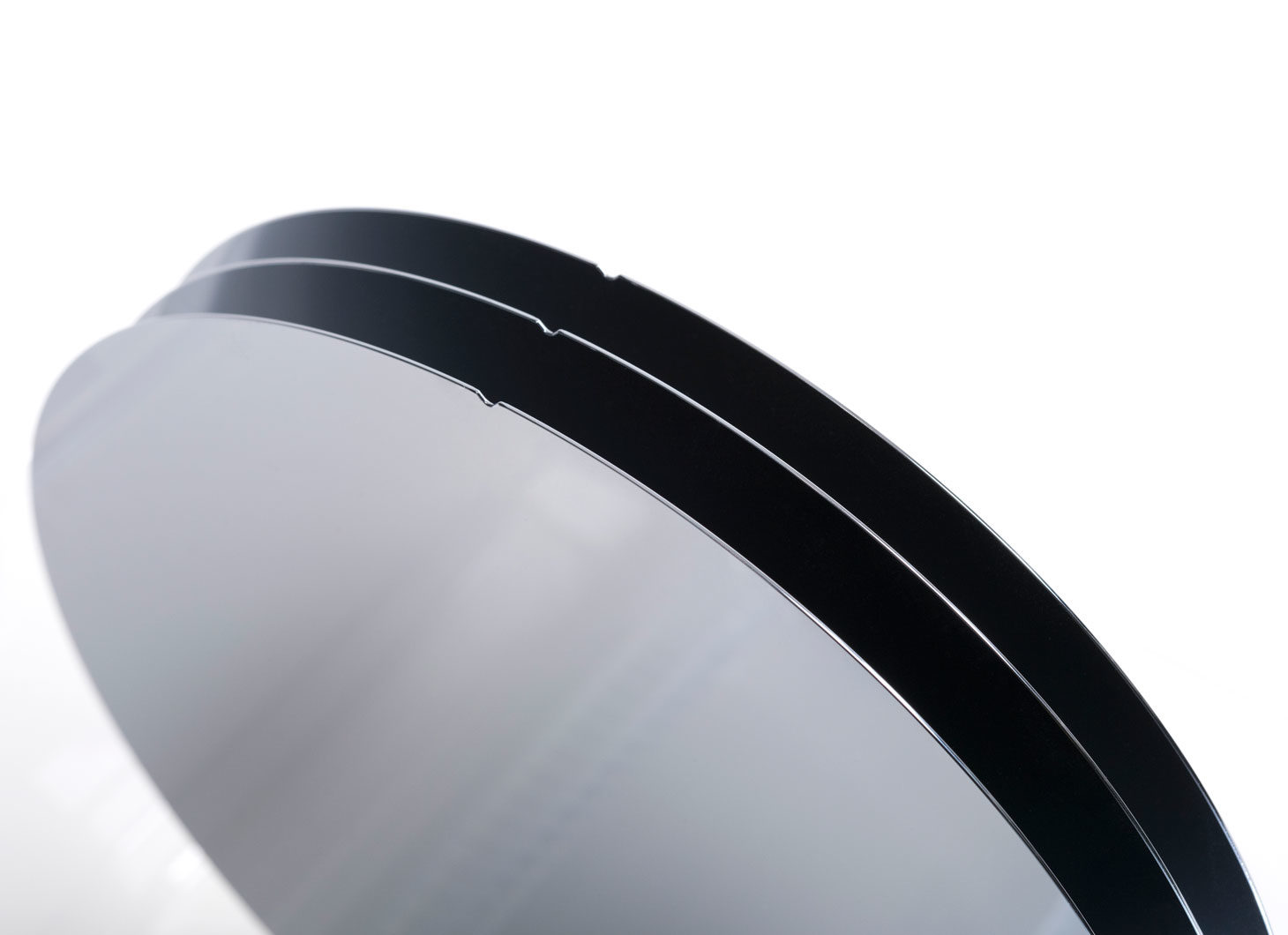
Okmetic introduces an Enhanced SOI wafer (E-SOI) into its SOI product family (Silicon-On-Insulator). Because of its new level of layer thickness uniformity and unprecedented properties E-SOI is an ideal platform for demanding applications such as HV BCD devices, silicon photonics and high-precision silicon-based MEMS sensors.
The device layer thickness of E-SOI is freely adjustable between 1.0 µm and >100 µm and the thickness tolerance independent of target thickness is as low as +/-0.1 µm. With the wide selection of silicon starting materials from Okmetic’s in-house crystal growth, and similar flexibility in wafer customization as Okmetic BSOI wafers, the E-SOI technology provides an ideal wafer solution to both semiconductor and sensor applications.

