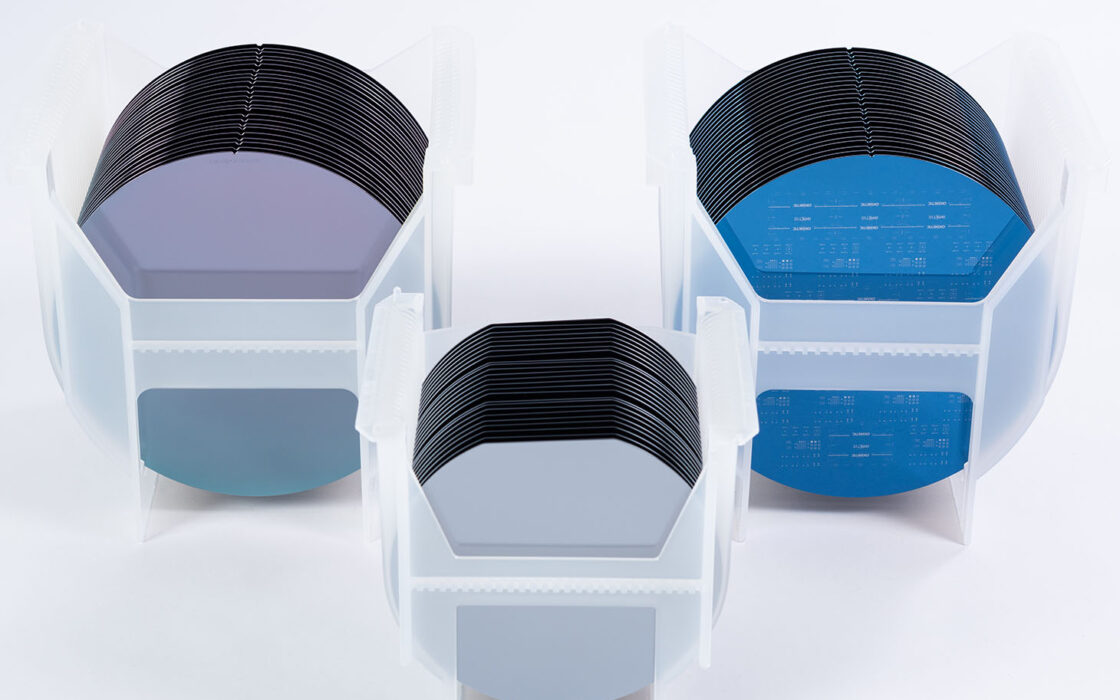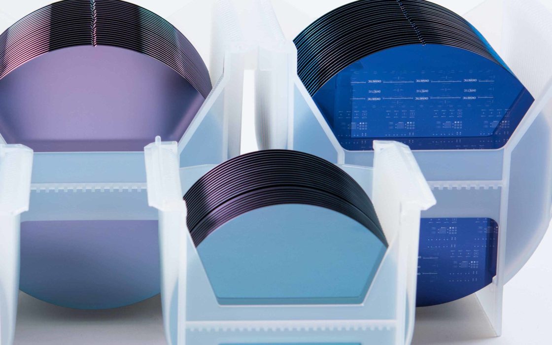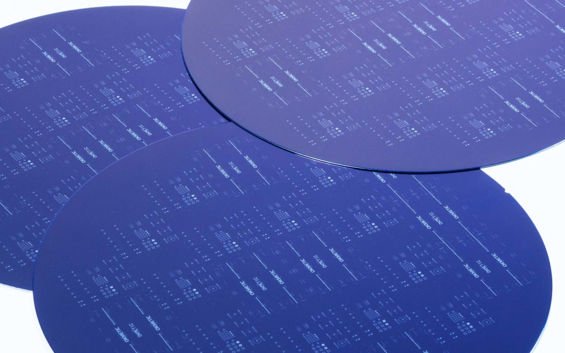
DSP wafers – Double Side Polished
Okmetic has been supplying Double Side Polished DSP wafers since 1985 and today they are used as a platform for surface MEMS, capping as well as RF and Power devices. Our DSP wafers are tailored to meet each customer’s process and product specific requirements. Available in 150-200 mm.
Okmetic is a pioneer as an advanced silicon wafer supplier for demanding semiconductor devices and DSP wafers have been in our product portfolio ever since our foundation. Okmetic has also been qualified DSP wafer supplier for the automotive industry ever since the 1990’s, which means that our DSP wafers have a long history in meeting the most stringent semiconductor quality standards. Okmetic 200 mm DSP production capacity will see a significant increase in early 2025, following the expansion of its Vantaa site fab.
Okmetic has been qualified DSP wafer supplier for the automotive industry since the 1990’s.
Our in-house crystal growing and wide selection of wafer materials enable the manufacture of customized DSP wafer solutions tailored to meet each customer’s process and product specific requirements. Our high-resistivity RFSi® wafer line includes DSP wafers designed for the needs of RF filters and devices. Power wafer line includes DSP wafers tailored for the needs of discrete power devices and GaN growth. MEMS wafer line includes DSP wafers optimized for the needs of surface MEMS and capping. These wafers are available with or without patterns. Many MEMS devices such as pressure sensors, accelerometers and gyroscopes are typically using DSP or SSP wafers as a platform, but the use of SOI wafers is on the increase for the sake of their cost-effectiveness.
Excellent thickness uniformity and orientation accuracy
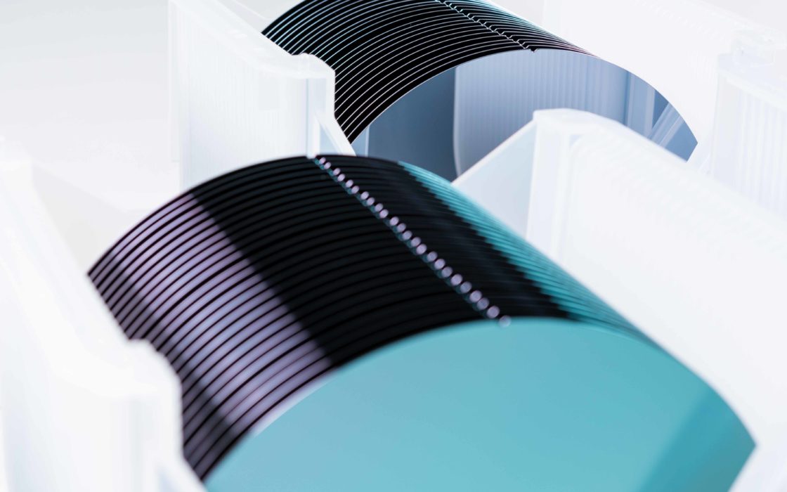
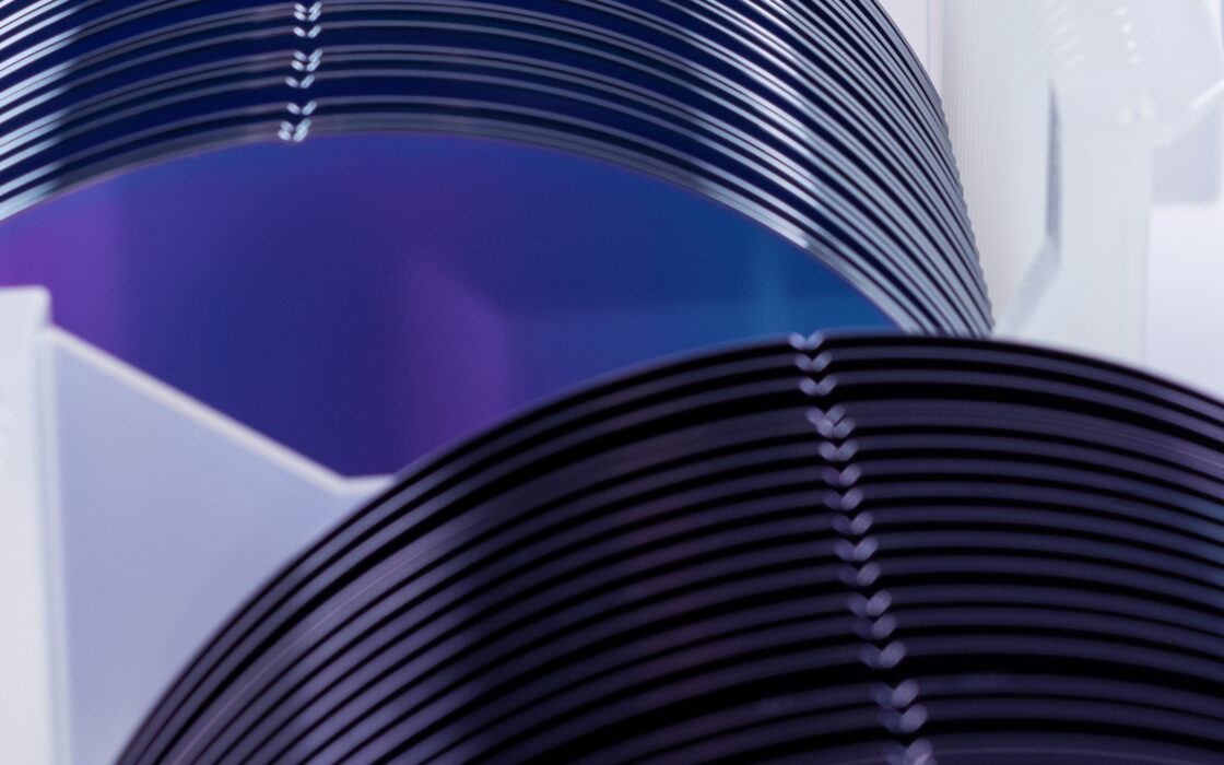
Okmetic’s extensive experience and know-how ensures that our Double Side Polished DSP wafers have excellent thickness uniformity and orientation accuracy, as well as first-rate crystal quality and homogeneity. Also our wide selection of wafer parameters enable highly customized DSP wafer solutions for a variety of device needs.
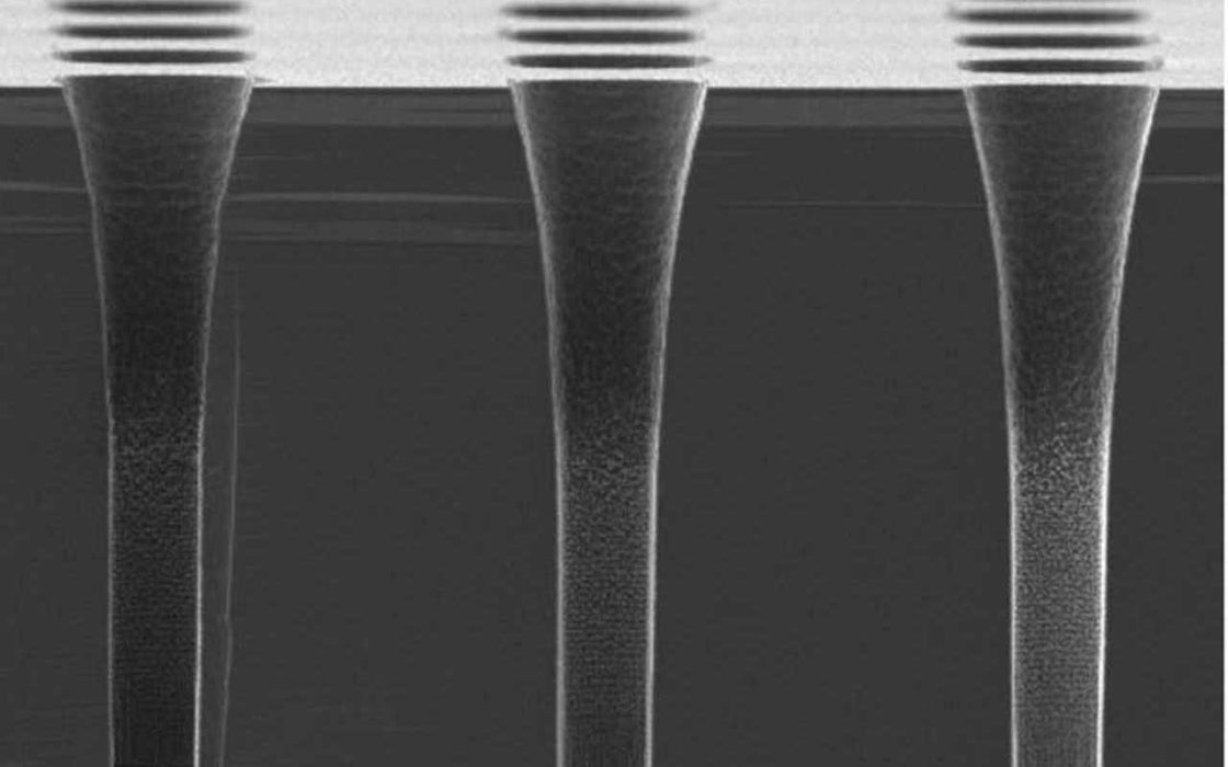
Our DSP wafers offer an excellent platform for double-sided lithography. Okmetic thin DSP wafers are optimized for fast processing, which have shown to lead to cost and quality benefits. Okmetic’s DSP wafers are also widely used as cap wafers in MEMS devices, providing excellent bonding strength and hermetic sealing of MEMS structures. DSP wafers optimized for bulk micromachining and alkali etching (e.g. KOH, TMAH) ensure high precision of the sensing elements, stable quality and effective processing.
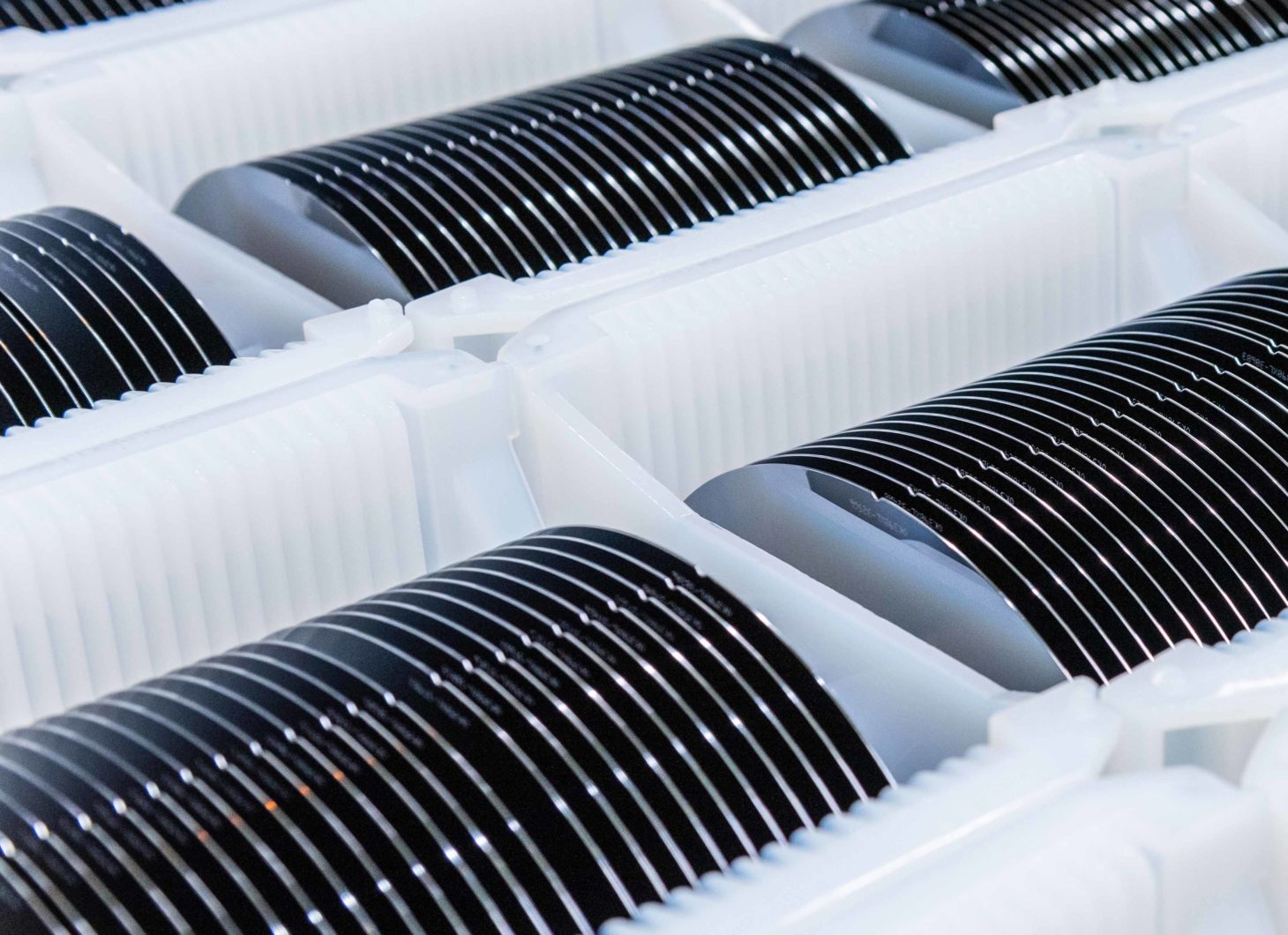
Okmetic has wide selection of 150 to 200 mm DSP silicon wafers. Wafer dopants include antimony, arsenic, phosphorus, and boron. Crystal orientation can be <100>, <110>, <111> or off-oriented. Thicknesses range from 380 to >1,150 µm and resistivities from <0.001 to >10,000 Ohm-cm.
DSP wafer specifications
| Growth method | Cz, MCz, A-MCz® |
| Diameter | 200 mm, 150 mm |
| Crystal orientation | <100>, <110>,<111>, off-oriented |
| N type dopants | Antimony, Arsenic, Phosphorus, Red Phosphorus |
| P type dopants | Boron |
| Resistivity1 | Between <0.001 and >10,000 Ohm-cm |
| Thickness2 | 200 mm: 380 to 1,150 µm 150 mm: 380 to >1,150 µm |
| Thickness tolerance3 | ±5 µm |
| TTV4 | <1 µm |
| Orientation accuracy5 | ±0.2° |
2Other thicknesses possible with certain limitations.
3±3 µm for demanding devices
4 Thickness limitations
5 ±0.15° for demanding devices
Fully CMOS compatible wafer surface quality and cleanliness requirements