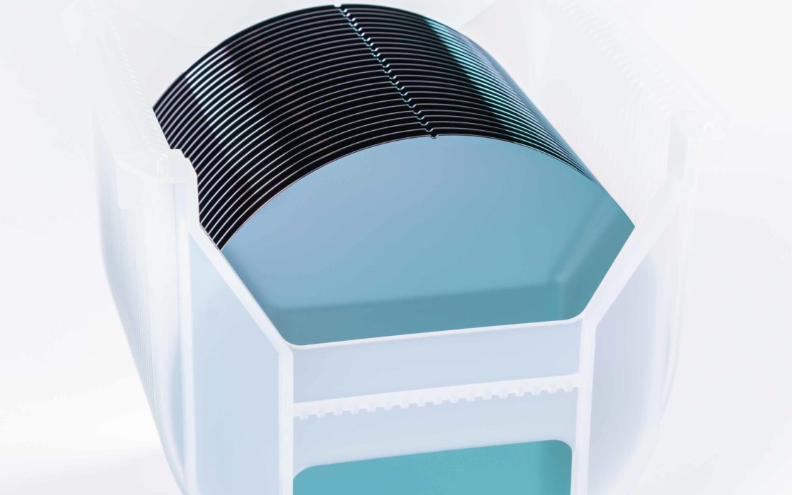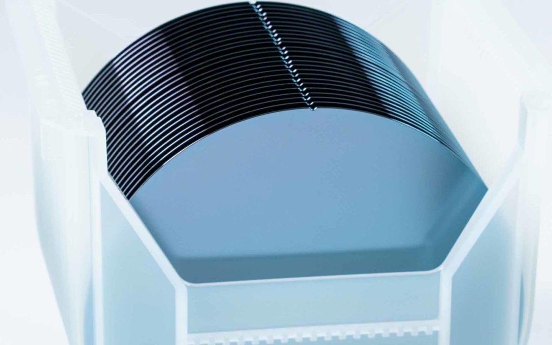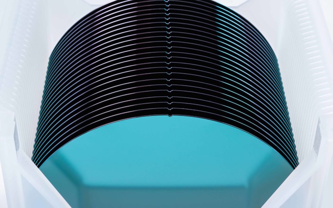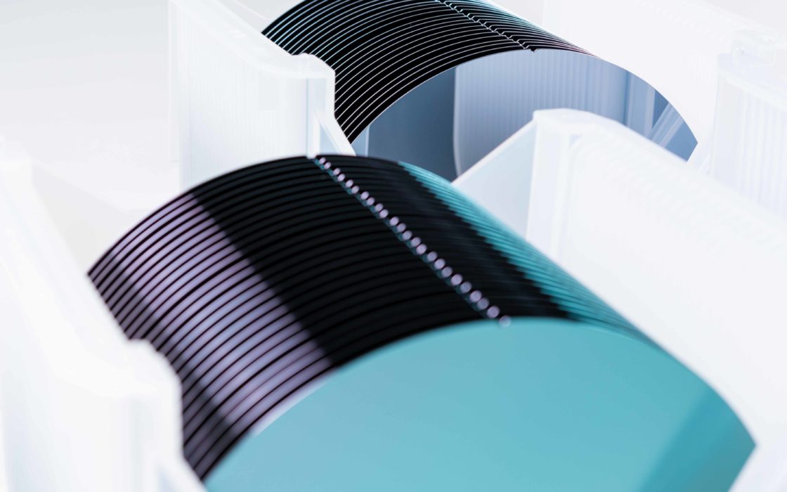
RF GaN Substrate wafers for GaN-on-Si applications
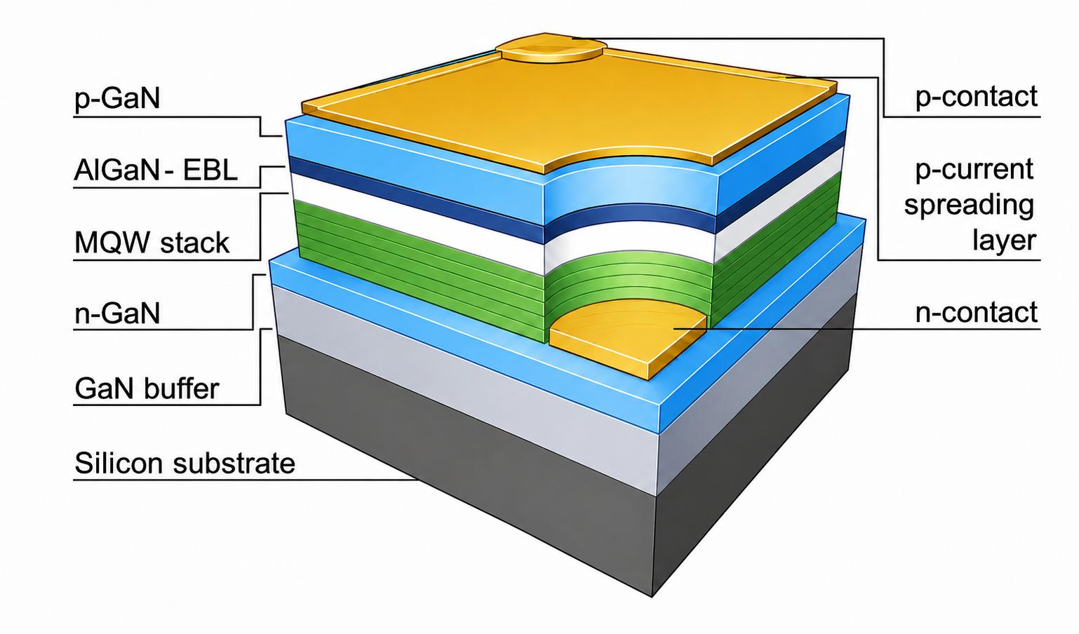
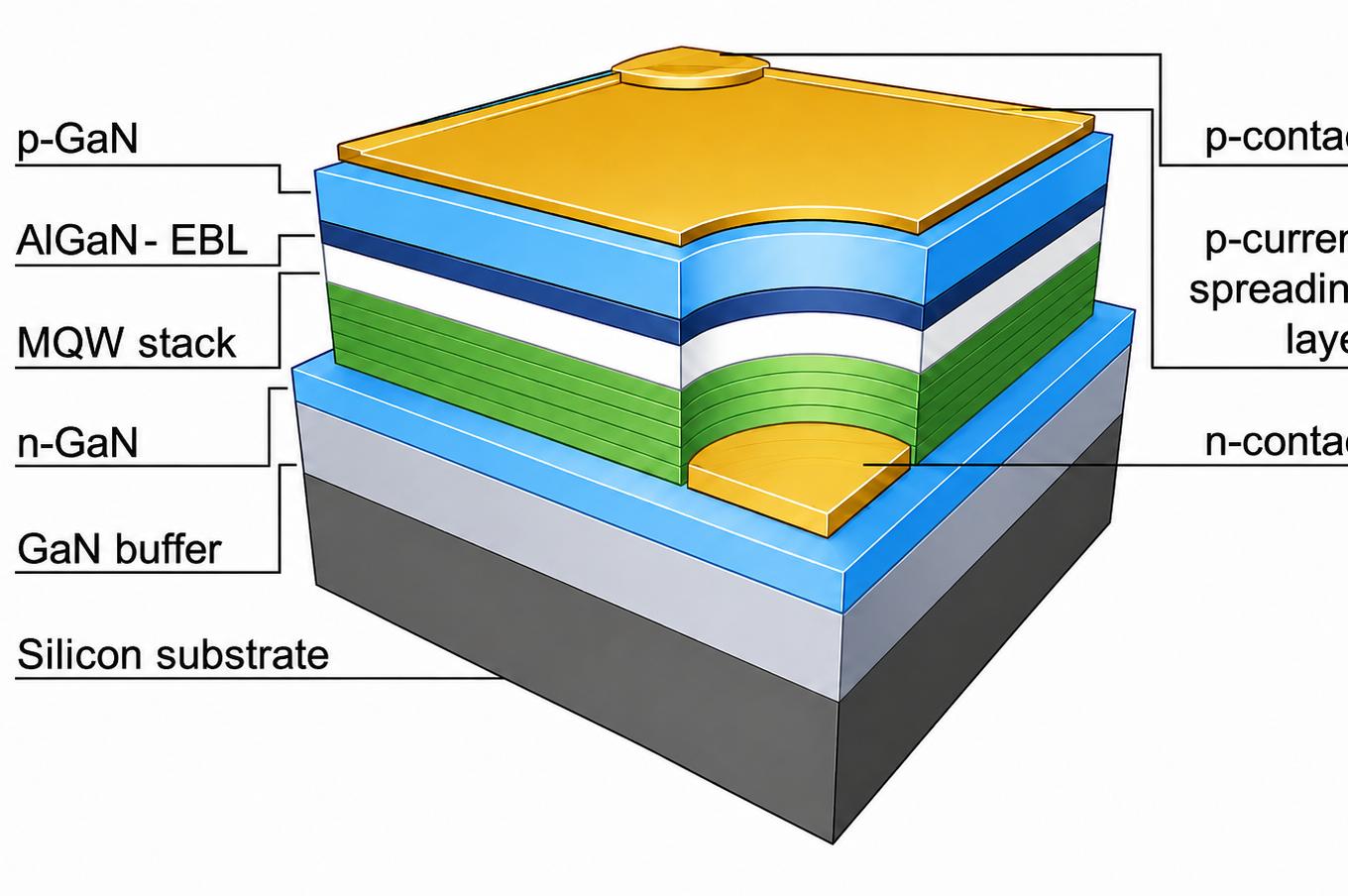
Okmetic RF GaN Substrate wafers are customized high resistivity silicon substrates engineered to support high-quality gallium nitride (GaN) epitaxy and low RF insertion losses. Optimized substrate properties help manage the mechanical and thermal stresses associated with GaN-on-Si growth, improving wafer stability during epitaxial processing.
Growing GaN on silicon creates significant mechanical and thermal stresses due to the lattice and thermal mismatch between GaN and silicon. Okmetic RF GaN Substrate wafers are engineered to support demanding GaN epitaxy through optimized wafer thickness, oxygen concentration, crystal orientation, and engineered wafer edges. High resistivity silicon, with options exceeding 10 kOhm-cm, helps minimize RF losses in the substrate, supporting low insertion losses and high-performance RF GaN devices.
Silicon wafers designed to endure the extreme stresses of the RF GaN epi process and to drive the insertion losses lower
Okmetic RF GaN Substrate wafers are a result of long-term silicon parameter optimization carried out in close co-operation with industrial partners across a wide range of GaN epitaxy processes. Okmetic also supplies silicon and SOI substrates for power GaN applications, including medium and low resistivity silicon wafers for GaN-on-Si and GaN-on-SOI. Find out more about Okmetic GaN Substrate wafer benefits from our White paper: Enabling next-gen power and RF GaN devices with optimized silicon and SOI substrates.
Optimized silicon substrates for high-quality GaN epitaxy
Wafer thickness is an important parameter in managing mechanical stability during GaN epitaxy. Okmetic offers a wide range of customized wafer thicknesses up to 1,150 µm, as well as a variety of backside treatment options, enabling the substrate to be optimized for different GaN epitaxy processes. Increased wafer thickness can help reduce in-situ curvature and manage wafer bow and warpage during GaN growth.
Okmetic RF GaN Substrate wafers are available in <111> crystal orientation with tight orientation control to support consistent GaN epitaxy. Controlled interstitial oxygen (Oi) concentration enhances mechanical strength and slip resistance during high-temperature processing and can be optimized according to customer process requirements. Engineered wafer edges help optimize gas flow and thermal distribution during GaN epitaxy.
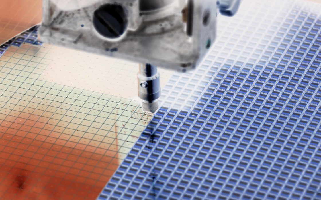
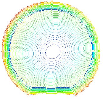
Okmetic silicon wafers have consistently demonstrated stable performance in GaN-on-Si epitaxy. In the example shown, the Okmetic wafer bow returns close to its initial level after GaN stack deposition. This is illustrated in the geometrical mapping of an Okmetic Si substrate processed into a GaN-on-Si wafer at Aalto University in Finland. Full-wafer shape analysis can complement in-situ wafer monitoring and support systematic optimization of the epitaxial process.
RF GaN Substrate wafers have multiple benefits
- Tailored substrate properties to meet demanding GaN epitaxy requirements
- High resistivity silicon, with options exceeding 10 kOhm-cm, supports low RF insertion losses.
- <111> crystal orientation with tight orientation control supports consistent GaN epitaxy.
- Customized wafer thickness up to 1,150 µm helps manage wafer curvature, bow and warpage during GaN epitaxy.
- Controlled interstitial oxygen (Oi) enhances mechanical strength and slip resistance during high-temperature processing.
- Engineered wafer edges support optimized gas flow and thermal distribution during GaN epitaxy.
- Double Side Polished (DSP) wafers and customized backside treatment options are available to meet different process requirements.
Specifications of RF GaN Substrate wafers
| Growth method | MCz, A-MCz® |
| Diameter | 200 mm, 150 mm |
| Crystal orientation | <111> |
| N type dopants | Phosphorus |
| P type dopants | Boron |
| Resistivity | Up to >7,000 Ohm-cm*, Available also in Ultra High Resistivity version with >10 kOhm-cm resistivity *Resistivity range varies by dopant and orientation |
| Oxygen | Typically ≤5 ppma or ≤10 ppma (ASTM F121-83). Can be optimized to Customer process. |
| SSP wafer thickness | 200 mm: 550 to 1,150 µm* 150 mm: 400 to 1,150 µm *Other thicknesses possible with certain limitations |
| DSP wafer thickness | 200 mm: 380 to 1,150 µm* 150 mm: 380 to >1,150 µm *Other thicknesses possible with certain limitations |
| Backside treatment | Etched, LTO, Polyback |
See all 150-200 mm silicon wafers