Photonics co-operation reference: VTT finds Okmetic E-SOI® wafers highly beneficial platform for its Photonics Technology
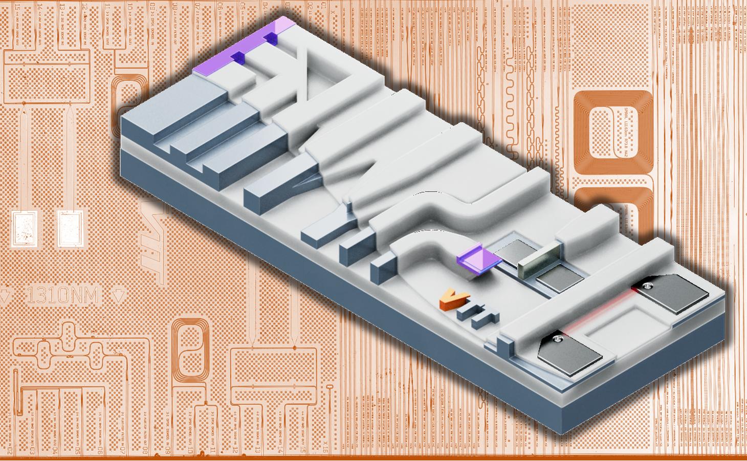
Picture Courtesy of VTT: VTT Photonics Technology featuring 3µm Okmetic E-SOI® platform with 3µm box and Ge PD with evaluation die background
VTT is a visionary research, development and innovation partner and one of the leading research organisations in Europe. The organisation develops photonic integrated circuits (PICs) and chips, which enable new components and systems for telecommunication, healthcare, autonomous vehicles and space applications. VTT’s PICs give the highest integration density based on patented design. Okmetic has been co-operating with VTT since early 2010s to develop an optimized wafer platform for their photonics technology needs.
E-SOI® wafer provides excellent waveguide for Silicon Photonics
VTT has opted to use Okmetic E-SOI® wafers with thick and highly uniform device/waveguide layer as a platform for its Photonics Technology instead of e.g. SOI wafers with submicron device layer.
This is because the E-SOI® wafers with thick and highly uniform device layer properties offer an excellent waveguide for silicon photonics. The E-SOI® wafer platform enables all-around high-performance optical solution with minimal or no polarization sensitivity, superior wavelengths range and highest tolerance to optical power. VTT PICs use device/waveguide layer thickness of 3µm, which is quite common for photonics devices.
Main benefits of VTT 3µm PIC using E-SOI® wafer as a platform:
- Single-mode operation with over 1.2 – 6 µm wavelength
- High integration density
- Extremely low optical losses down to less than 0.04dB/cm (measured through whole PIC)
- Small or zero polarization dependency
- Tolerance to high optical powers
Read more about VTT’s Silicon photonics technology here.