Apply for our Production Expert position
Are you looking for a unique and stable job that gives you the freedom to plan your free time in advance? We are seeking motivated individuals to work in production. Are you ready to become a top-notch silicon wafer expert building a better tomorrow?
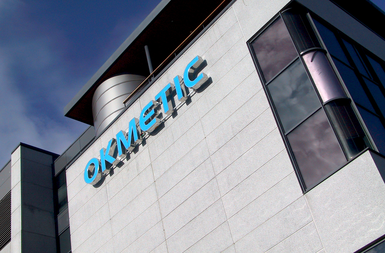
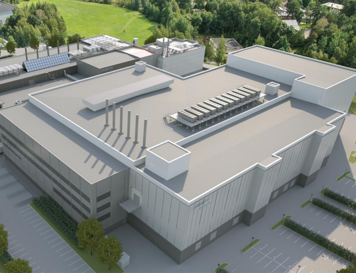
Vantaa’s Koivuhaka Fab: Home to Silicon Wafer Experts
You will have an important role in our technology-forward production, working in continuous shift production.
Although previous experience is not required, the silicon wafer manufacturing process involves many work stages that require precision and diligence as well as basic IT skills.
In this position, we expect that you communicate fluently in Finnish. English is considered an advantage.
More freedom and flexibility in your life
With our shiftwork model, you can experience a new level of freedom and flexibility in your life as you know your upcoming work schedules well in advance.
Developed in collaboration with our employees, you will enjoy more days off than workdays in a month. That’s right – imagine having more time to do the things you love.
The cycle starts with two morning shifts (7 am–7 pm), followed by a day off, two night shifts (7 pm–7 am), and finally five days off.

Become a top-notch expert with our training program
During the 2–6 month induction period, you will have a personal coach by your side to support you. The induction program is based on the requirements related to quality, environment and safety in industrial work.
We can quickly train our personnel to adapt to new product areas and meet changing demand and customer requirements, ensuring a stable and reliable job both now and tomorrow.

Get paid based on your skills and experience
Our employees receive compensation based on collective agreements, with personal increments from day one. As you gain competence, your personal performance will influence your personal increment, which can be an additional 5–26% on top of your basic pay.
In addition to the hourly wage, you will be paid a shift increment and a monthly production bonus that is based on meeting the common production targets.

Our people are the heart of our technology
We strongly value our employees, recognizing that each person plays an important role in our success.
In addition to occupational healthcare services, we offer recreational activities, a company bike benefit, a culture and exercise benefit, and assistance with caring for a sick child. We even have our own gym.

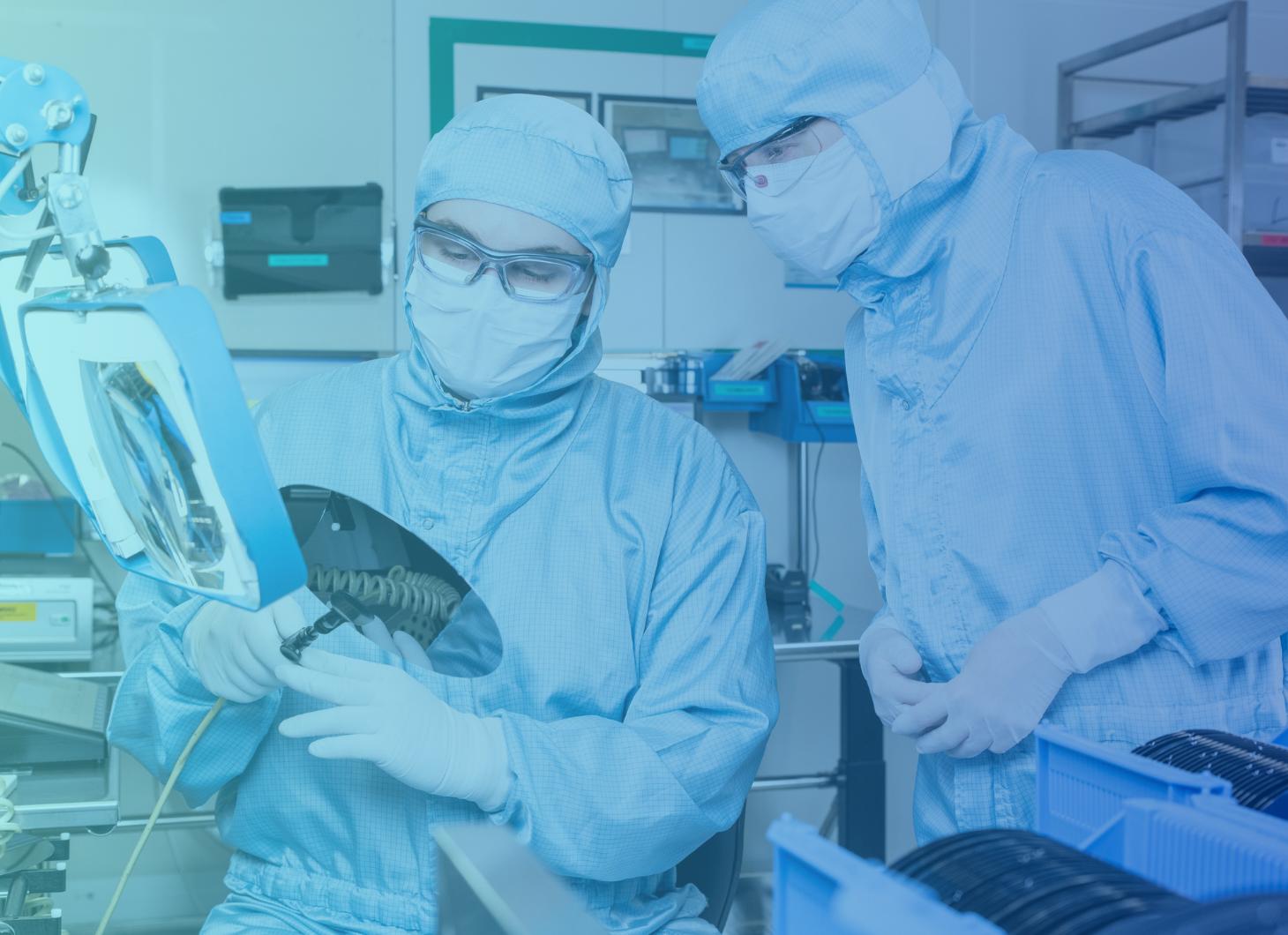
Discover the fascinating world of silicon wafer manufacturing
Don’t just take our word for it – let’s hear it from Sonja Viljanen, a Okmetic employee for over 17 years.
From start to finish, each stage of the process offers a unique challenges. With a wide range of tasks and daily challenges, Sonja finds her job both exciting and fulfilling. Whether you are familiar with silicon wafers or not, Okmetic provides a supportive and engaging work environment.
Are you Sonja’s next colleague?
- Manufacturing process starts with crystal growing: High-purity, semiconductor-grade silicon is melted in a crystal growing furnace and grown into a single crystal. The crystal is then cut into smaller sections for further processing. The work involves controlling and monitoring the furnace processes as well as assisting with the different stages of these processes.
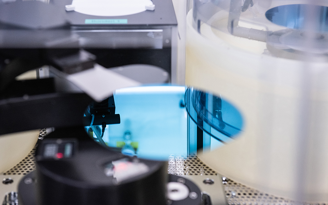
- The crystal is cut into wafers: Silicon ingots are taken into wafering facilities where they are sliced into wafers. Other tasks include various measurements and adjustments as well as taking care of operator-based equipment maintenance.
- Significant part of the process takes place in the clean room: Big part of the process takes place in the clean room, since the most important quality criterion is cleanliness. There are a number of stages in wafer processing that take place in cleanrooms of different classes. Silicon wafer batches are processed further, washed and inspected using a variety of automatic or semi-automatic equipment.
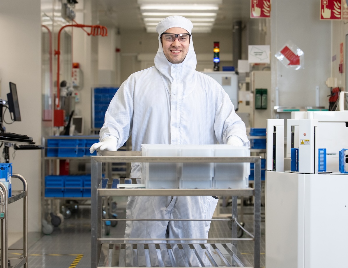
- After packaging the wafers are sent to the customers: The processing of silicon wafers often involve various further processing steps. Finally, the wafers are inspected, packaged, and delivered to the customer as a raw material for the manufacture of MEMS, sensors, RF devices, or power devices.
Get to know our top-notch experts


Join us on our journey!
By 2025, we will complete a fab expansion that is expected to double the production capacity and business and create over 500 new jobs.
Despite fluctuations in demand, we are a stable and reliable employer. Thanks to long-term contracts, a diverse product portfolio and accurate demand forecasting, we have successfully avoided workforce adjustments for over a decade.