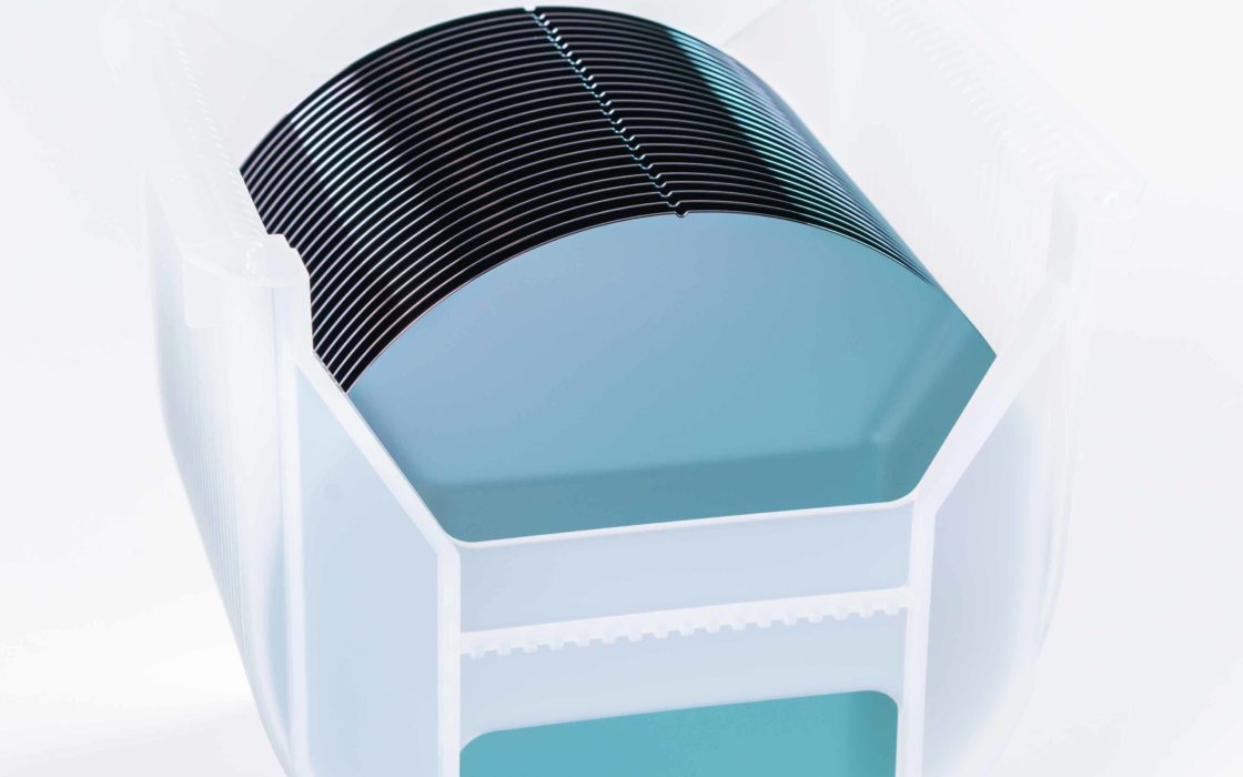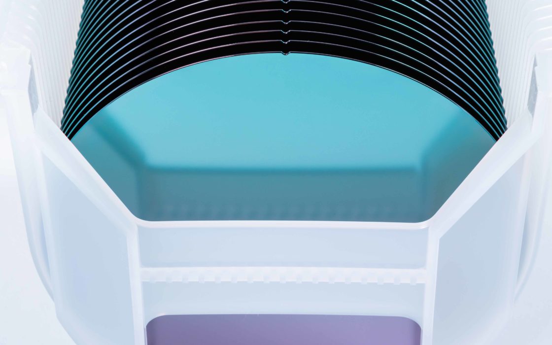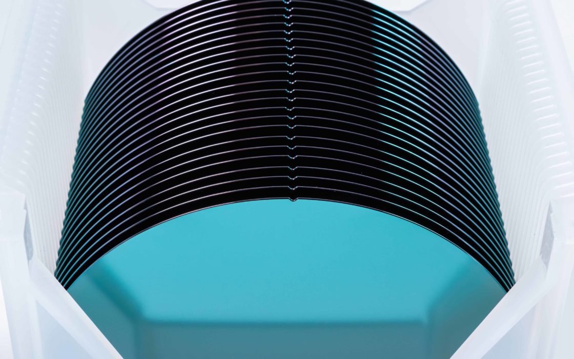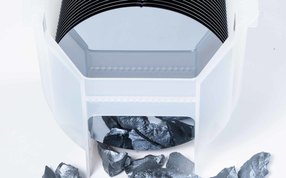
UF-RFSi® – Ultra Flat High Resistivity wafers
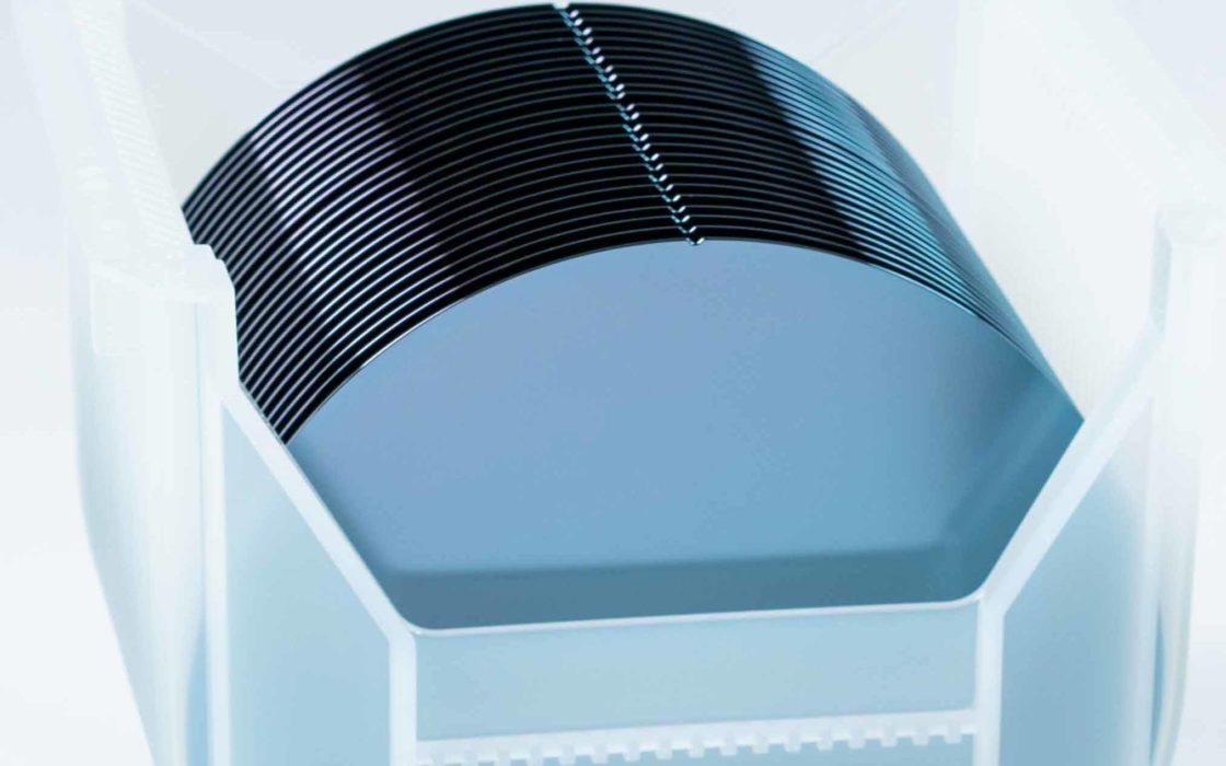
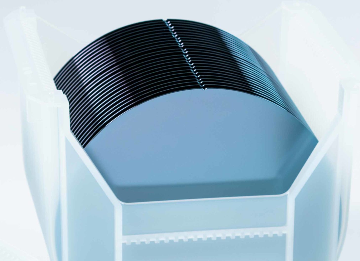
Okmetic UF-RFSi® wafer is an engineered high resistivity silicon wafer with ultra-flat properties optimized specifically for the needs of TF-SAW filters. UF-RFSi® wafer combines very low TTV with low Oi, up to >7,000 Ohm-cm resistivity and optional trap-rich layer.
UF-RFSi®is an engineered high resistivity silicon wafer dedicated for thin film surface acoustic wave (TF-SAW) hybrid structures. As the industry’s first high resistivity silicon wafer with ultra-flat geometries, UF-RFSi® leverages Okmetic’s proprietary Advanced Magnetic Czochralski (A-MCz®) crystal growth technology to deliver improved technical performance with high resistivity for ultra low-loss radio frequency (RF) specifications. The Ultra Flat High Resistivity silicon wafer enables customers to achieve the most challenging active layer geometries. Additionally, the design flexibility makes the wafer a high performance and cost-effective solution for demanding filter and RF technology. Find out more about our Engineered high resistivity wafer benefits in our White paper “Advancing from 4G LTE to 5G and 6G: Engineered RFSi® silicon wafers for high-performance RF devices.
UF-RFSi® wafer improves RF performance and enables the manufacture of challenging active layer geometries cost-effectively.
Optimized for TF-SAW filters
UF-RFSi® wafers provide and optimal platform for e.g. TF-SAW filters as it features more efficient planarization of the device layer in addition to stable resistivity, low insertion loss and superior linearity performance when compared to competitive offerings. The ultra-flat high resistivity wafer boasts a Total Thickness Variation (TTV) below 700 nm and very low non-circular symmetry variation, which enables more efficient planarization of the device layer with less trimming steps required in bond and grind back process. This results to significant reduction in investments at the customer end.
UF-RFSi® wafer’s below 700 nm TTV reduces need for further trimming
The ultra-flat wafer can undergo a fully customizable wafering process in terms of crystal and flat orientations and optional engineered trap-rich layer that help maximize gains in harmonic behavior and overall losses. Our customers benefit from tailored solutions that are optimized to meet their specific product, process and technology needs.
UF-RFSi® wafer specifications
| Growth method | MCz, A-MCz® |
| Diameter | 150 mm, 200 mm |
| Crystal orientation | <100>, <111> |
| N type dopants | Phosphorus |
| P type dopants | Boron |
| Resistivity | Up to >7,000 Ohm-cm*, available also in Engineered Ultra High Resistivity version with >10 kOhm-cm resistivity *Resistivity range varies by dopant and orientation |
| Oxygen | Typically ≤5 ppma or 5 – 10 ppma (ASTM F121-83). Can be optimized to Customer process. |
| SSP wafer thickness | 200 mm: 550 to 1,150 µm* 150 mm: 400 to 1,150 µm *Other thicknesses possible with certain limitations |
| DSP wafer thickness | 200 mm: 380 to 1,150 µm* 150 mm: 380 to >1,150 µm *Other thicknesses possible with certain limitations |
| TTV | Below 700 nm |
| Trap-rich layer (optional) | Purely silicon-based, no foreign materials |
| Back surface | SSP etched, DSP polished |
UF-RFSi® stands for performance, freedom of design and reduced investments
- High resistivity combined with very low TTV (below 700nm) and non-circular symmetry variation.
- Simplified manufacturing of hybrid structures through better planarization efficiency.
- Improved RF performance achieved with more efficient planarization, stable resistivity, low insertion loss, and superior linearity performance.
- Optional, highly efficient purely silicon-based trap-rich layer on top of the wafer to maximize the gains in harmonic behavior and overall losses.
- UF-RFSi® can be customized for customer design enabling optimized configurations or new wave modes to be used in Thin Film SAW devices