Engineered silicon substrates for microLED manufacturing
Achieving consistent epitaxial quality and high manufacturing yield are key challenges in GaN-on-Silicon microLED manufacturing, placing stringent requirements on both the epitaxial process and the underlying silicon substrate. Engineered silicon wafers can provide the controlled substrate properties and mechanical stability needed to support uniform GaN epitaxy and scalable microLED production.
High brightness, low power consumption, fast response time and the potential for extremely high resolution make microLED technology attractive for applications including microdisplays and AR/VR devices, wearable electronics and advanced consumer displays.
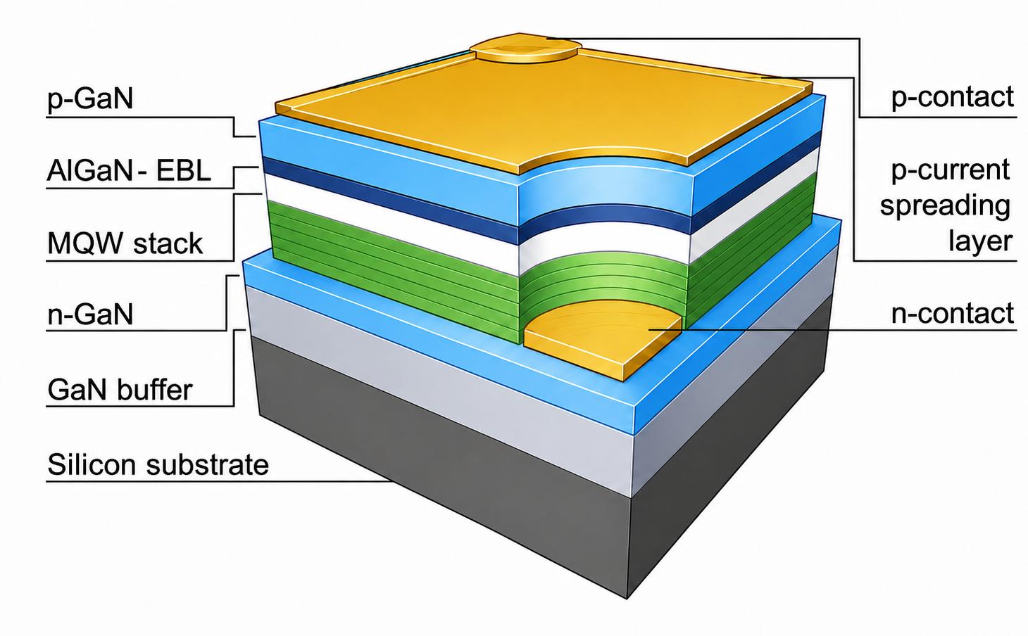
Most blue and green microLEDs are based on InGaN/GaN epitaxial structures grown by metal–organic chemical vapor deposition (MOCVD). Their emission wavelength and intensity depend on the composition and properties of the active region and the quality of the epitaxial layers. Even small variations in composition, thickness, or quality of epitaxial layers can result in visible differences in color and brightness across a microLED display, making highly uniform epitaxial growth essential. For GaN-on-Silicon microLEDs, this places stringent requirements on the underlying silicon substrate.
Silicon substrate requirements for MicroLED epitaxy
GaN epitaxy for microLED manufacturing requires excellent emission wavelength uniformity across a single wafer, from wafer to wafer and between epitaxial growth runs. This is particularly important because LEDs originating from different wafers and growth runs may ultimately be integrated into the same display.
Unlike conventional LED manufacturing, wavelength binning is generally not feasible in the same way due to the mass-transfer process. This increases the importance of controlling wavelength and intensity variation already during epitaxial growth.
The silicon substrate is one of the factors influencing the conditions for high-quality GaN epitaxy. For GaN-on-silicon microLED manufacturing, important substrate considerations include crystal orientation and off-cut tolerance, wafer thickness, oxygen concentration, surface quality and defectivity. Together, these parameters influence epitaxial quality and the mechanical stability of the wafer during high-temperature processing.
Optimizing off-cut for epitaxial and wavelength uniformity
The silicon wafer off-cut angle, also referred to as the substrate miscut angle, strongly influences the step density, terrace width and step orientation of the substrate surface. Optimizing the off-cut is important, as the resulting step structure can influence surface roughness and step bunching during GaN epitaxy, affecting epitaxial morphology and uniformity.
In microLED applications, off-cut can also have implications for wavelength uniformity. Surface step morphology can influence indium incorporation in the InGaN active region and thereby affect the emission wavelength. Both an optimized target off-cut and a tight off-cut tolerance are important for supporting consistent epitaxial growth and wavelength uniformity, ultimately contributing to consistent color performance.
Mechanical stability during high-temperature GaN epitaxy
The thermal expansion mismatch between GaN and silicon generates stress during high-temperature MOCVD processing and subsequent cooling. This can contribute to post-epitaxial bow and warp as well as slip and crack formation. Controlling these effects is important for subsequent microLED fabrication processes and manufacturing yield.
Both wafer thickness and silicon crystal properties can be engineered to improve mechanical stability during GaN epitaxy. Wafer thickness can be optimized to provide sufficient rigidity and help control wafer curvature under epitaxial stress. Interstitial oxygen concentration (Oi) is another important parameter. Optimized Oi levels increase the resistance of silicon wafers to slip formation during high-temperature processing.
Key silicon substrate parameters for MicroLED epitaxy
For GaN-on-silicon microLED epitaxy, substrate selection focuses primarily on parameters affecting epitaxial quality, thickness uniformity and mechanical stability rather than on a specific resistivity requirement.
Key silicon substrate considerations include:
- crystal orientation <111> with an off-cut optimized for the epitaxial process
- tight off-cut tolerance
- high surface quality and low defectivity
- wafer thickness optimized for mechanical stability and curvature control
- optimized interstitial oxygen concentration for improved slip resistance
The maturity of silicon wafer technology and its compatibility with established semiconductor manufacturing infrastructure make silicon an attractive platform for scalable GaN microLED manufacturing. Okmetic’s engineered silicon wafers can be tailored for demanding GaN epitaxy, with key substrate parameters optimized to support epitaxial uniformity, mechanical stability and scalable microLED manufacturing.
Interested in learning more about silicon substrate optimization for GaN epitaxy?
Explore our white paper on optimized silicon and SOI substrates for GaN power and RF devices.
Read the GaN substrate white paper