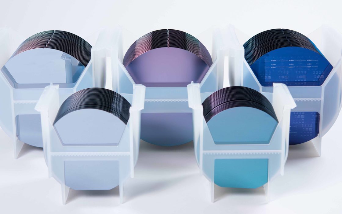
300 mm Polished silicon wafers
Okmetic provides 300 mm polished silicon wafers for advanced semiconductor manufacturing, supporting foundries, OSATs, and IDMs across memory, power, RF, and digital and analog ICs.
Okmetic provides 300 mm polished silicon wafers for advanced semiconductor manufacturing, supporting foundries, OSATs, and IDMs across memory, power, RF, and digital and analog ICs. Our 300 mm wafer portfolio is produced through qualified manufacturing partners. Okmetic retains full responsibility for supply chain management and wafer quality, ensuring a smooth and reliable order-to-delivery process.
This model ensures consistent prime-grade wafer quality, reliable delivery performance, and tailored substrate solutions for device fabrication, advanced packaging, and heterogeneous integration technologies, including TSV, interposers, and HBM.
Near Perfect Silicon wafers
COP-free wafers with low defectivity (at LLS 19 nm) and excellent GOI performance. Customizable Oi concentration between 7-14 ppma and resistivity between 1-250 Ohm-cm. Also high BMD option available. Well suited for 2D/3D NAND, DRAM, NOR Flash, BCD (PMIC), TSV, and carrier wafers.
Argon Annealed wafers
Argon Annealed wafers with COP-free zone ≥8 µm and BMD DZ ≥20 µm. High BMD density (1E9 ~ 1E10/cm3) for effective gettering efficiency and mechanical strength. Well suited for display driver ICs (DDIC), HV CMOS, and embedded flash (eFlash).
TSV and Carrier wafers
Low COP, low Oi, and low BMD wafers featuring a customized edge profile to minimize edge chipping induced by bonding and thinning. Well suited for TSV, 2.5D/3D packaging, interposers, HBM, and CIS carrier wafers.
IGBT wafers
Low Oi (<5 ppma), low carbon (<0.06 ppma), low COP (<500 counts at LLS 37 nm) wafers with customizable resistivity (1-300 Ohm-cm). RRG and ROG capability <6%. Well suited for IGBT and FRD applications.
Non-Standard wafers
Thick wafers (775-1000 µm), thin wafers (600-775 µm) and reduced diameter wafers (298-300 mm). Both <100> and <111> orientations available. Well suited for 3D NAND, GaN substrates and special test wafers.
<111> Orientation Polished wafers
Wafers with low COP density and superior mechanical strength. Resistivity range 0.002-1,000 Ohm-cm. Wafer thicknesses up to 1,000 μm. Well suited for RF GaN substrates, power devices and microLEDs, 3D NAND, and SOI donor wafers.
High Resistivity wafers
High resistivity wafers with poly layer for parasitic surface conduction suppression and improved linearity. High performance in second harmonics, insertion loss, intermodular distortion and Q values. Low Oi concentration (<5 ppma). Well suited for RF devices and IPDs.
N++ Polished wafers
Arsenic doped wafers with ≥1.8 mOhm-cm resistivity and Red phosphorus doped wafers with ≥0.8 mOhm-cm resistivity. Well suited for Power MOSFETs, SGT MOSFETS and SJ MOSFETS.
P++ Polished wafers
Boron doped wafers with ≥1.3 mOhm-cm resistivity. Well suited for Power MOSFETs, SGT MOSFETS and SJ MOSFETS.