EPI wafers – Epitaxial silicon wafers
High-quality EPI wafers (epitaxial silicon wafers) provide a perfect platform for power discretes, power management ICs, optical components and MEMS devices. Available in 100-200 mm.
Okmetic manufacturing partners’ EPI wafers and epitaxial services complement Okmetic wafer portfolio. Okmetic in charge of supply chain management and quality of the silicon epitaxial wafers guarantees smooth Order-Delivery process.
Two service models
- Okmetic-manufactured silicon substrates available in 150-200 mm with partner’s epitaxial layer
- Fully partner-manufactured silicon EPI wafers available in 100-200 mm
EPI wafer features
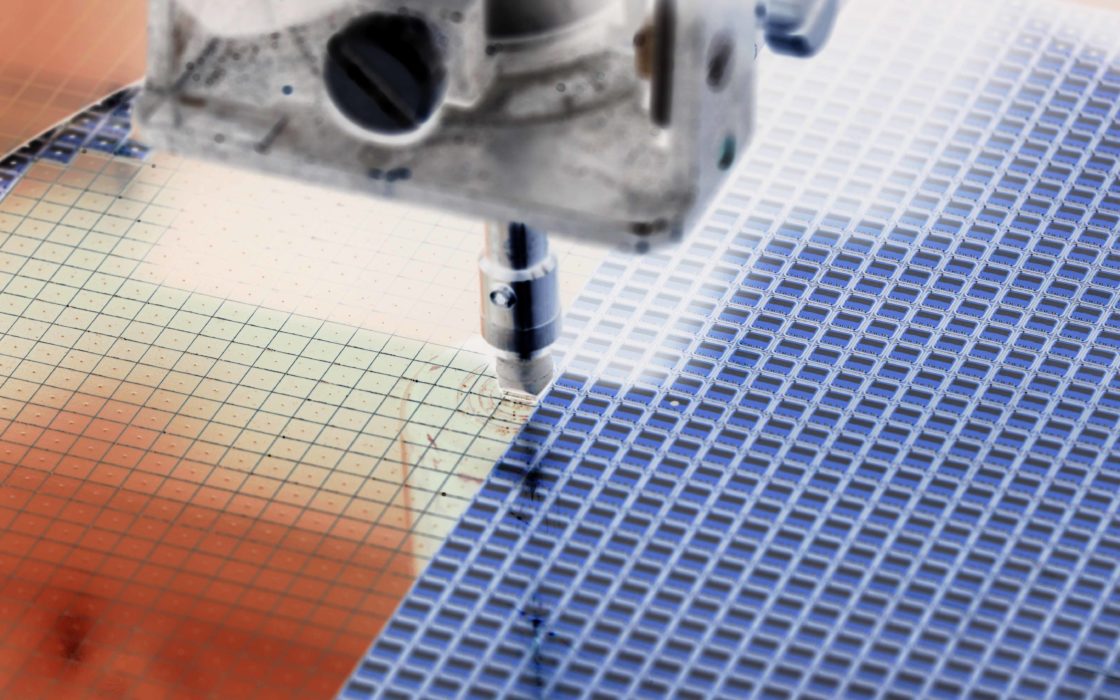
The following characteristics of silicon EPI wafers define the material and interface performance for advanced device processing.
- Excellent EPI layer thickness uniformity for precise membrane dimensional control
- Sharp EPI-to-substrate interface
- High material quality and purity
Okmetic EPI substrate features
Okmetic 150-200 mm silicon EPI substrates can be customized for customer needs. Resistivities range from <0.001 up to >10,000 Ohm-cm. Available wafer thicknesses range from 380 µm up to 725 µm. The wafers feature excellent thickness uniformity, flatness, and orientation accuracy. Backside treatments include polished, etched, and polyback. Wafers can have a customized wafer edge refined for the customer’s process. There is also a possibility to process backside alignment marks. Learn more about SSP substrates and DSP substrates.
Epitaxy features for EPI wafers
EPI wafers (silicon epitaxial wafers) feature tight control of epitaxial layer thickness and resistivity uniformity across supported wafer sizes. The epitaxial layers are available with boron, phosphorus, and arsenic doping, enabling a wide range of resistivity targets.
The EPI process delivers low metal contamination levels (<3E10 atoms/cm²) and a sharp, well-defined EPI-to-substrate interface, contributing to high material purity and layer quality.
EPI silicon wafers feature tight control of epitaxial layer thickness and resistivity uniformity across supported wafer sizes.
EPI layer thickness options vary by wafer type and diameter, ranging from , 1–180 µm for 150–200 mm SSP EPI wafers, 1–15 µm for 150–200 mm DSP EPI wafers used for MEMS devices, and up to 3–180 µm for 100–125 mm SSP EPI wafers. Thickness uniformity is specified down to ≤1.0–1.2%. Resistivity uniformity is specified at ≤2.2% for low-resistivity layers and ≤5% for higher-resistivity layers.
Multi-layer epitaxy capability supports complex device structures and advanced integration requirements for power, optical, and MEMS device applications.
Okmetic EPI substrate wafer specifications
| Growth method | Cz, MCz, A-MCz® |
| Diameter | 200 mm, 150 mm |
| Crystal orientation | <100>, <110>,<111>, off-oriented |
| Orientation accuracy1 | ±0.2° |
| N type dopants | Antimony, Arsenic, Phosphorus, Red Phosphorus |
| P type dopants | Boron |
| Resistivity2 | Between <0.001 and >10,000 Ohm-cm |
| SSP wafer thickness3 | 200 mm: 625 to 725 µm 150 mm: 400 to 625 µm |
| DSP wafer thickness3 | 200 mm: 625 to 725 µm 150 mm: 380 to 625 µm |
| Thickness tolerance4 | ±5 µm |
| TTV5 | <1 µm |
1 ±0.15° for demanding devices
2 Over 1,500 Ohm-cm is possible with P-type boron doping. Resistivity range varies by dopant and orientation.
3 Other thicknesses possible with certain limitations
4 ±3 µm for demanding devices
5 Thickness limitations
Fully CMOS compatible wafer surface quality and cleanliness requirements
Epitaxy specification for 150-200 mm SSP wafers
Metal <3E10 atoms/cm2.
| EPI resistivity | EPI thickness | EPI dopant | Thickness uniformity | Resistivity uniformity |
| 0.015-3,600 Ohm-cm | 1-180 µm | Boron | ≤1.0% for ≤20 EPI thickness, 1.5% for ≥20 EPI thickness | ≤2.2% (Resistivity ≤20 Ohm-cm) ≤5% (Resistivity ≥20 Ohm-cm) |
| 0.035-330 Ohm-cm | 1-180 µm | Phosphorus | ≤1.0% for ≤20 EPI thickness, 1.5% for ≥20 EPI thickness | ≤2.2% |
| 0.005-0.5 Ohm-cm | 1-20 µm | Arsenic | ≤1.0% for ≤20 EPI thickness, 1.5% for ≥20 EPI thickness | ≤2.2% |
Epitaxy specification for 100-125 mm SSP wafers
Available 100-125 mm substrate thicknesses are 450-525 µm. Metal <3E10 atoms/cm2.
| EPI resistivity | EPI thickness | EPI dopant | Thickness uniformity | Resistivity uniformity |
| 0.04-3,600 Ohm-cm | 3-180 µm | Boron | ≤1.0% for ≤20 EPI thickness, 1.5% for ≥20 EPI thickness | ≤2.2% (Resistivity ≤20 Ohm-cm) ≤5% (Resistivity ≥20 Ohm-cm) |
| 0.05-330 Ohm-cm | 3-180 µm | Phosphorus | ≤1.0% for ≤20 EPI thickness, 1.5% for ≥20 EPI thickness | ≤2.2% (Resistivity ≤20 Ohm-cm) ≤5% (Resistivity ≥20 Ohm-cm) |
Epitaxy specification for 150-200 mm DSP wafers
Metal <3E10 atoms/cm2.
| EPI resistivity | EPI thickness | EPI dopant | Thickness uniformity | Resistivity uniformity |
| 0.015-100 Ohm-cm | 1-15 µm | Boron | ≤1.2% | ≤2.2% (Resistivity ≤20 Ohm-cm) ≤5% (Resistivity ≥20 Ohm-cm) |
| 0.035-10 Ohm-cm | 1-15 µm | Phosphorus | ≤1.2% | ≤2.2% |
| 0.005-0.5 Ohm-cm | 1-15 µm | Arsenic | ≤1.2% | ≤2.2% |
See all 150-200 mm silicon wafers