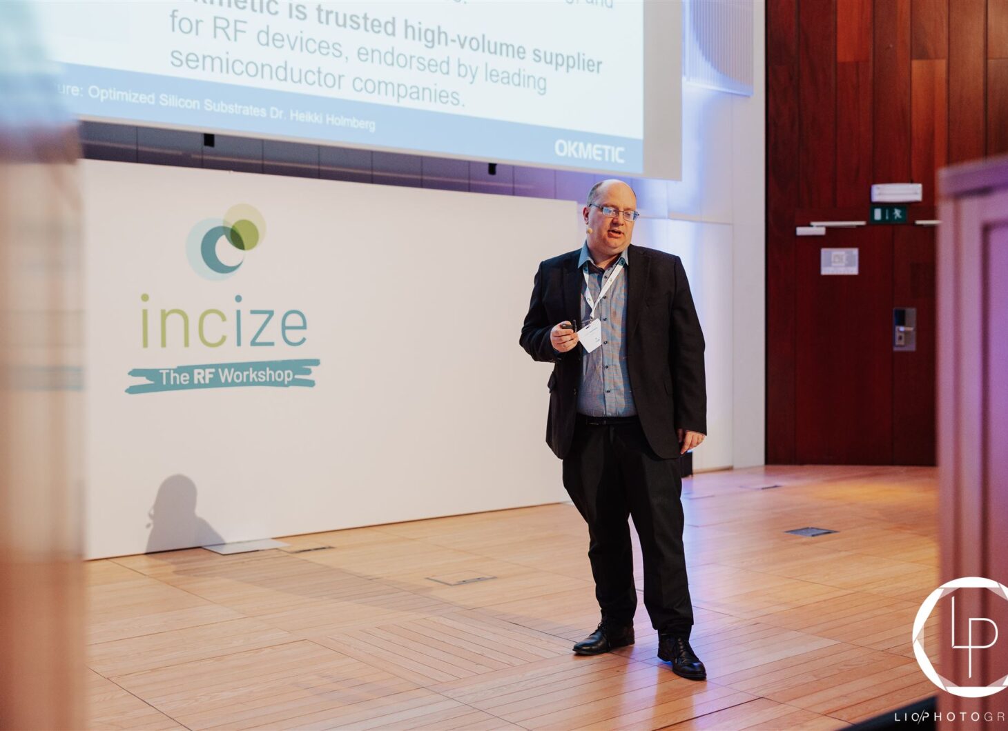
R&D Director Heikki Holmberg speaking at Incize RF Workshop
Our R&D Director, Dr. Heikki Holmberg, presenting at the RF workshop hosted by Incize on 24 April.
The event provided a valuable platform for technical exchange across the RF ecosystem, bringing together industry experts to discuss enabling next-generation RF performance.
During the workshop, Holmberg shared insights on how engineered silicon substrates help address key challenges in GaN-based RF and 5G/6G applications.
Key highlights:
• Engineered High Resistivity Silicon wafers reduce RF losses, enhance resonator Q, and enable high-linearity RF designs
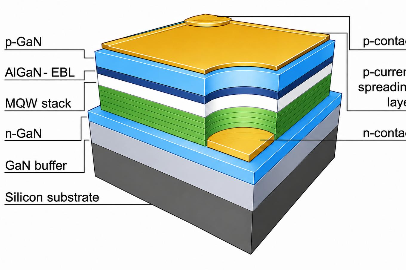
• Optimized silicon substrates for GaN-on-Si provide a scalable, cost-efficient platform for high-performance RF applications
• SOI substrates for GaN-on-SOI with deep-trench isolation enable integration, reduce parasitic coupling, and support complex GaN ICs
For a more in-depth technical perspective, explore our latest whitepapers on GaN substrate and Engineered High Resistivity silicon wafer solutions.