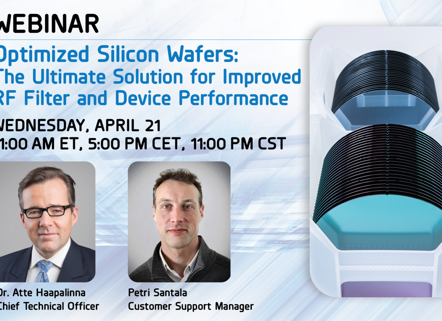
Upcoming Webinar – Optimized Silicon Wafers: The Ultimate Solution for Improved RF filter and Device Performance
Join our webinar on Wednesday, April 21 11:00AM ET, 5:00PM CET, 11:00 PM CST
5G and the wider bands, lower latency, greater connectivity and higher frequencies are setting new performance standards for RF filters and other RF devices. There is also added pressure on new product innovations to overcome the mobile industry’s interference challenges and more stringent parameter requirements.
Join us on April 21 to learn more about the latest substrate trends in the RF market and discover Okmetic’s industry leading portfolio of high resistivity RFSi™ wafers for:
- Acoustic wave filters
- IPD devices
- Power amplifiers
- Integrated RFIC power amplifiers
- Silicon interposers
Read more and register now (link is external)
The presenters
Dr. Atte Haapalinna is chief technical officer at Okmetic, the leading supplier of advanced silicon wafers. He has published two dozen papers on various applications of advanced silicon substrates, silicon damage characterization and silicon photodetectors. Dr. Haapalinna has been with Okmetic since 1998, holding various positions including senior vice president of products, senior vice president of customer support and senior manager of new business development. He has participated in development of C-SOI® substrates, ultra-low resistivity power applications and engineered high resistivity materials for RF applications. Dr. Haapalinna received his Ph.D. at the Helsinki University of Technology (now Aalto University), Finland.
Mr. Petri Santala is the customer support manager at Okmetic. He is responsible for technical customer support in North America, which has gained him vast expertise on RF manufacturers’ needs and optimized wafer solutions. Mr. Santala has over 20 years of experience in silicon-based material engineering. He has worked for Okmetic since 1999 and held various positions related to research and development, process engineering and quality and applications support. In recent years, he has also been actively involved in SEMI Manufacturing Working Group’s substrate standardization work and has spoken at various semiconductor events. Mr. Santala received his bachelor’s degree in process engineering at the Espoo University of Applied Sciences, Finland.


