Silicon wafer manufacturer for advanced semiconductor applications
What is a silicon wafer manufacturer? A silicon wafer manufacturer produces silicon substrates used as the starting material for semiconductor device fabrication. These wafers are used in technologies such as logic and memory integrated circuits, MEMS, RF devices, power electronics, and photonics.
Silicon wafers form the foundation of semiconductor device fabrication and are used across a wide range of technologies requiring high material precision and process stability. Their role is critical in enabling device integration, manufacturing yield, and long-term reliability across semiconductor applications.
Material properties such as crystal quality, resistivity, and surface quality directly influence device integration, manufacturing yield, and long-term reliability, making wafer manufacturing a critical part of the semiconductor value chain.
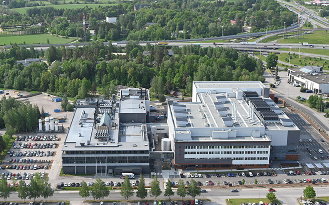
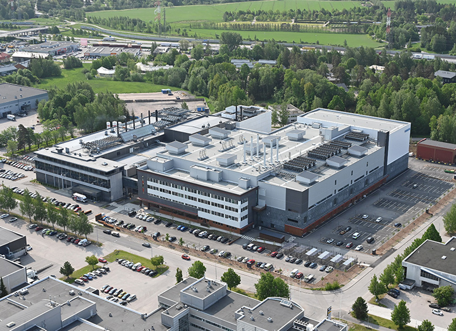
Okmetic is a silicon wafer manufacturer and supplier supplying silicon wafers for MEMS, RF, power, memory, logic and mixed IC devices. The company focuses on 150–200 mm silicon wafers manufactured in-house, with additional 300 mm wafers supported through manufacturing partners.
Okmetic’s portfolio includes 150-200 mm High Resistivity RFSi® wafers, SSP and DSP wafers, bonded SOI and cavity SOI substrates, patterned wafers, and TSV wafers, complemented by partner-manufactured 300 mm polished and 100-300 mm epitaxial wafers.
Role of silicon wafer manufacturers in semiconductor manufacturing
Silicon wafer manufacturers play a critical role in enabling semiconductor fabrication through crystal growth, wafer processing, and substrate engineering. Their capabilities directly influence material consistency, process compatibility, and production scalability across diverse semiconductor technologies.
Differences between silicon wafer suppliers are typically reflected in engineering capability, manufacturing footprint, customization support, and collaboration with device development teams.
Types of silicon wafer manufacturers
Types of silicon wafer manufacturers can be broadly categorized as:
- High-volume manufacturers supporting mainstream semiconductor applications
- Specialty manufacturers focused on application-specific wafer solutions (e.g. MEMS, RF, power)
Customization capability varies between suppliers and is often a key differentiator in supplier selection.
How to choose a silicon wafer manufacturer
Selecting the right silicon wafer manufacturer or supplier is critical for achieving reliable device performance and long-term production stability. Supplier selection directly impacts not only performance and cost, but also development risk, yield stability, and long-term supply continuity. Cost considerations are typically evaluated through total cost of ownership rather than wafer price alone. When evaluating potential silicon wafer manufacturers, consider the following key factors:
- Manufacturing expertise: Capability to support device-specific wafer characteristics and integration requirements.
- Customization options and capabilities: Ability to tailor material properties, layer structures, and engineered features to match your device design and process needs.
- Process control and tolerances: Consistent wafer characteristics across production lots supporting predictable device performance, yield, and cost-efficiency in manufacturing.
- Long-term supply stability: Sufficient manufacturing capacity, reliable delivery, and long-term lifecycle support, helping reduce supply risk and overall cost.
- Engineering collaboration: Technical interaction supporting requirement definition, prototyping, device optimization, and integration into the customer’s manufacturing process.
- Quality systems: Certified quality and environmental systems ensuring process discipline and wafer traceability.
When to choose specialized silicon wafers
Specialized silicon wafers are typically selected when device performance depends on material properties such as resistivity, defectivity, or engineered substrate structures. This is common in applications where standard wafer specifications do not provide sufficient performance, integration, or reliability.
Applications such as MEMS, RF, and power devices often require tailored wafer specifications to achieve optimal performance, yield, and reliability.
In these applications, wafer selection and engineering are closely linked to device performance and manufacturing requirements.
Examples of application-specific wafer considerations:
- MEMS devices: How to select the ideal wafer for MEMS devices
- RF and connectivity applications: Engineered RFSi® wafers for high-performance RF devices
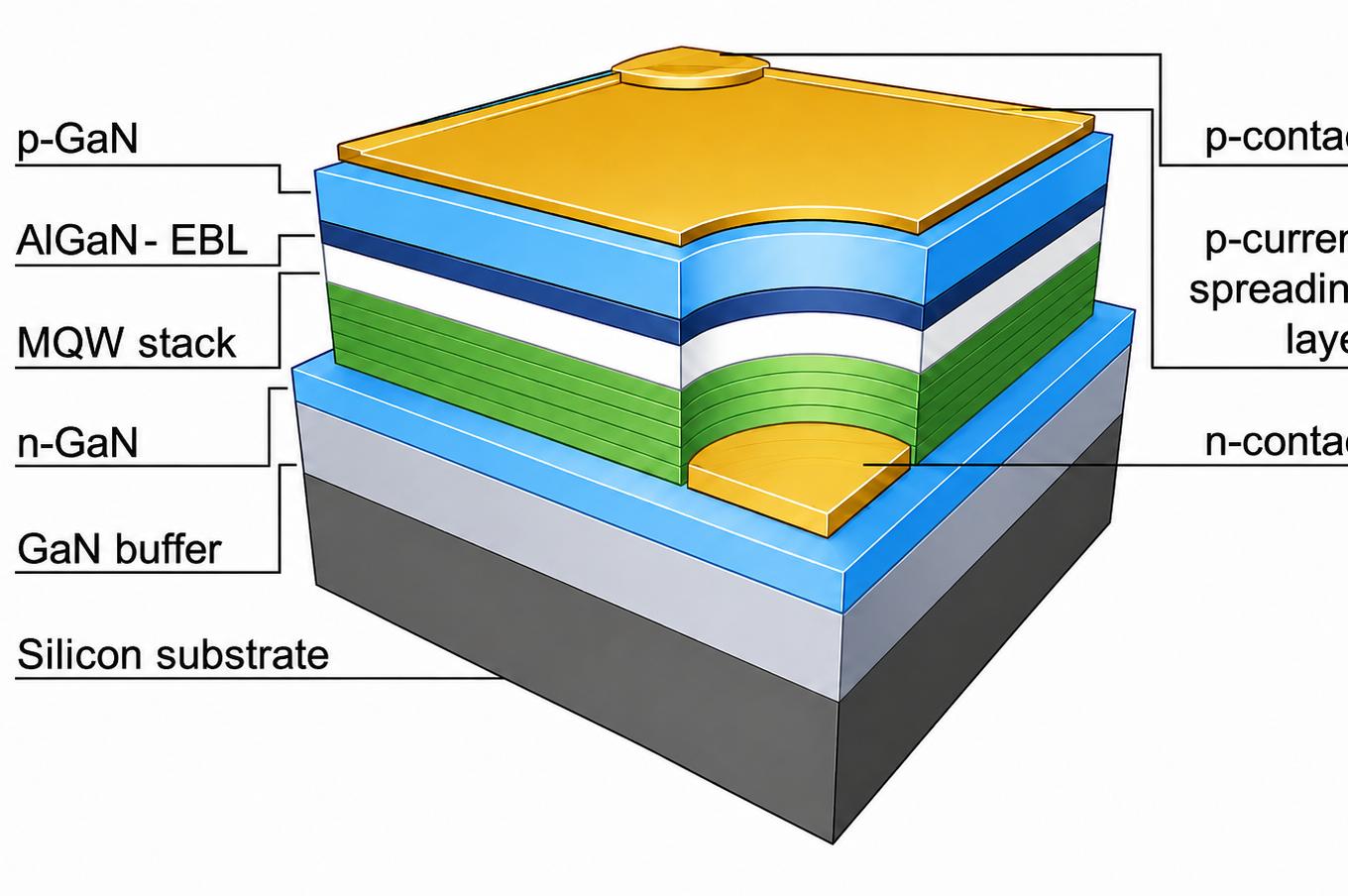
- Power and RF GaN devices: Optimized silicon substrates for next-generation power and RF GaN applications
Silicon wafer manufacturing capabilities
Silicon wafer manufacturing capabilities are based on crystal growth and wafer engineering, directly supporting semiconductor device performance and manufacturing efficiency.
Wafer size selection depends on application requirements, production scale, and technology node. While 300 mm wafers are widely used in high-volume logic and memory manufacturing, 150–200 mm wafers remain common in MEMS, RF, power, and a broad range of analog and industrial semiconductor applications.
As a silicon wafer manufacturer, Okmetic supports semiconductor device performance through advanced crystal growth and wafer engineering, offering customized silicon wafer solutions for demanding applications.
Wafer specifications
Okmetic’s capabilities include:
- Wafer diameters: 150-200 mm, 300 mm via manufacturing partners
- Growth methods: CZ, MCz, A-MCz®
- Crystal orientation: <100>, <110>, <111>, off-oriented
- N-type dopants: arsenic, antimony, phosphorus, red phosphorus
- P-type dopants: boron
- Resistivity: <1 mOhm-cm up to >10,000 Ohm-cm
- Thickness: 380 to >1150 μm, other thicknesses possible with certain limitations
- Backside treatment: etched, polyback, LTO, polished
Advanced manufacturing technologies
- CZ, MCz and A-MCz® crystal growth expertise across high and low resistivity wafers
- Trap-rich and engineered device layers
- Advanced wafer bonding technologies (Bonded Silicon-On-Insulator, Cavity SOI)
- Lithography and DRIE-enabled cavities, TSVs
- Defect and impurity control
Supported applications
Okmetic supplies silicon wafers used in semiconductor devices across a wide range of end applications, including:
- Automotive electronics
- Industrial electronics
- Medical and healthcare applications
- Consumer electronics and IoT
- Telecommunications and connectivity infrastructure
- Data centers and high-performance computing
- Artificial intelligence
- Aerospace and defence
- Renewable energy and electrification
These applications place different requirements on wafer properties such as resistivity, surface quality, and substrate structure.
Quality and sustainability
Silicon wafer manufacturing relies on controlled processes, certified quality systems, and long-term supply capabilities to ensure consistent material performance and availability across semiconductor applications.
Okmetic’s operations are based on certified quality systems and responsible manufacturing practices, supporting traceability, process stability, and long-term supply readiness, as described on Okmetic’s quality and sustainability pages.
Frequently asked questions (FAQ)
What does a silicon wafer manufacturer do?
A silicon wafer manufacturer produces silicon wafers used as the starting material for semiconductor device fabrication.
Do silicon wafer manufacturers offer custom silicon wafers?
Many semiconductor wafer suppliers, including Okmetic, offer silicon wafers that can be customized to match customers’ device and process requirements. However, the level of customization and engineering support can vary between manufacturers.
Okmetic collaborates with customers to define wafer requirements and ensure material properties align with device and process needs throughout the product lifecycle. This includes joint development, prototyping and ramp-up support, long-term supply planning, and engineering collaboration to maintain consistent wafer performance and process compatibility.
What sizes of silicon wafers are available?
Silicon wafers are commonly available from 100 mm to 300 mm, depending on silicon wafer manufacturer capabilities. Okmetic supplies silicon wafers primarily in the 150–200 mm range, with additional 300 mm wafers available through partner manufacturing.
What types of silicon wafers are available?
Silicon wafers can be grown using different crystal growth methods such as Czochralski (CZ), Magnetic Czochralski (MCz), Advanced Magnetic Czochralski (A-MCz®) and Float Zone (FZ). There are a variety of wafer types on the market including polished wafers, Silicon-On-Insulator wafers, epitaxial wafers, and high‑purity specialty wafers designed for advanced semiconductor manufacturing.
Okmetic focuses primarily on CZ, MCz, and A‑MCz® wafers, offering them in a variety of configurations tailored to customers’ device and process requirements. Okmetic’s portfolio includes 150-200 mm High Resistivity RFSi® wafers, SSP and DSP wafers, Bonded SOI and Cavity SOI substrates, patterned wafers, and TSV wafers, complemented by partner-manufactured 300 mm polished and 100-300 mm epitaxial wafers.
What benefits do high value-added silicon wafers offer?
They support enhanced device performance and reliability, improved manufacturing yield and process stability, and reduced total cost of ownership in advanced semiconductor applications.
Why choose Okmetic as your silicon wafer
Okmetic supplies silicon wafers for semiconductor applications requiring consistent material performance, process compatibility, and long-term supply stability. Okmetic’s core strength lies in specialty silicon wafers in the 150–200 mm range, where application-specific material engineering and customization play a critical role in device performance.
Key characteristics of Okmetic’s offering include:
- Focus on MEMS, sensor, RF, power, logic, memory and mixed signal ICs
- Expertise in crystal growth and wafer processing technologies
- Capability to support customized wafer specifications
- Scalable manufacturing for both high-volume and lower-volume needs
- Manufacturing in the 150–200 mm range, with additional 300 mm supply through partners
- Long-term collaboration with semiconductor customers
Contact a silicon wafer manufacturer
Semiconductor companies evaluating wafer suppliers may benefit from early engagement to optimize material selection and reduce development risk.
Early engagement with a silicon wafer manufacturer or supplier can support material selection, process alignment and reduced development risk.
Contact Okmetic to discuss technical requirements or request a quotation.