News
Select content category

Jaska Tuominen is appointed Senior Vice President, Human Resources, Sustainability and Communications
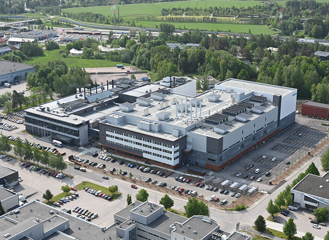
First silicon wafers out from Okmetic new Vantaa fab expansion
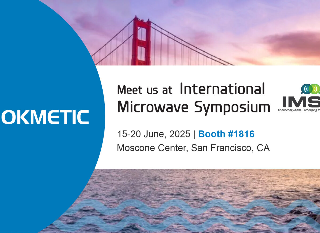
Okmetic participating in International Microwave Symposium

Okmetic attending PCIM Europe and SENSOR+TEST
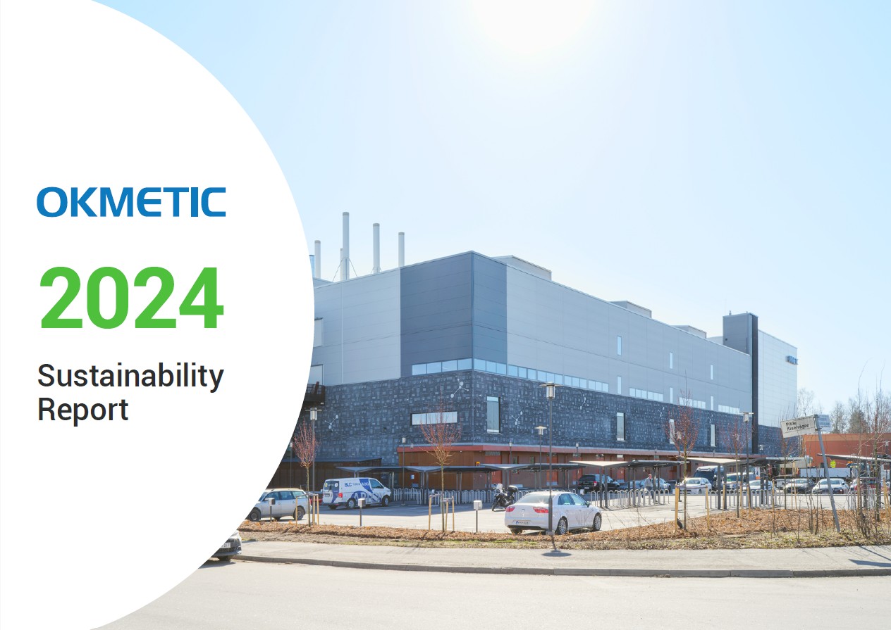
The Sustainability Report for 2024 has been published
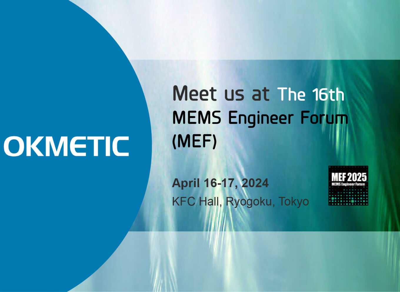
Okmetic participating in MEMS Engineer Forum
Okmetic achieved the highest Platinum level in a sustainability audit
20 years of C-SOI®: Enabling streamlined production of high-performance MEMS devices
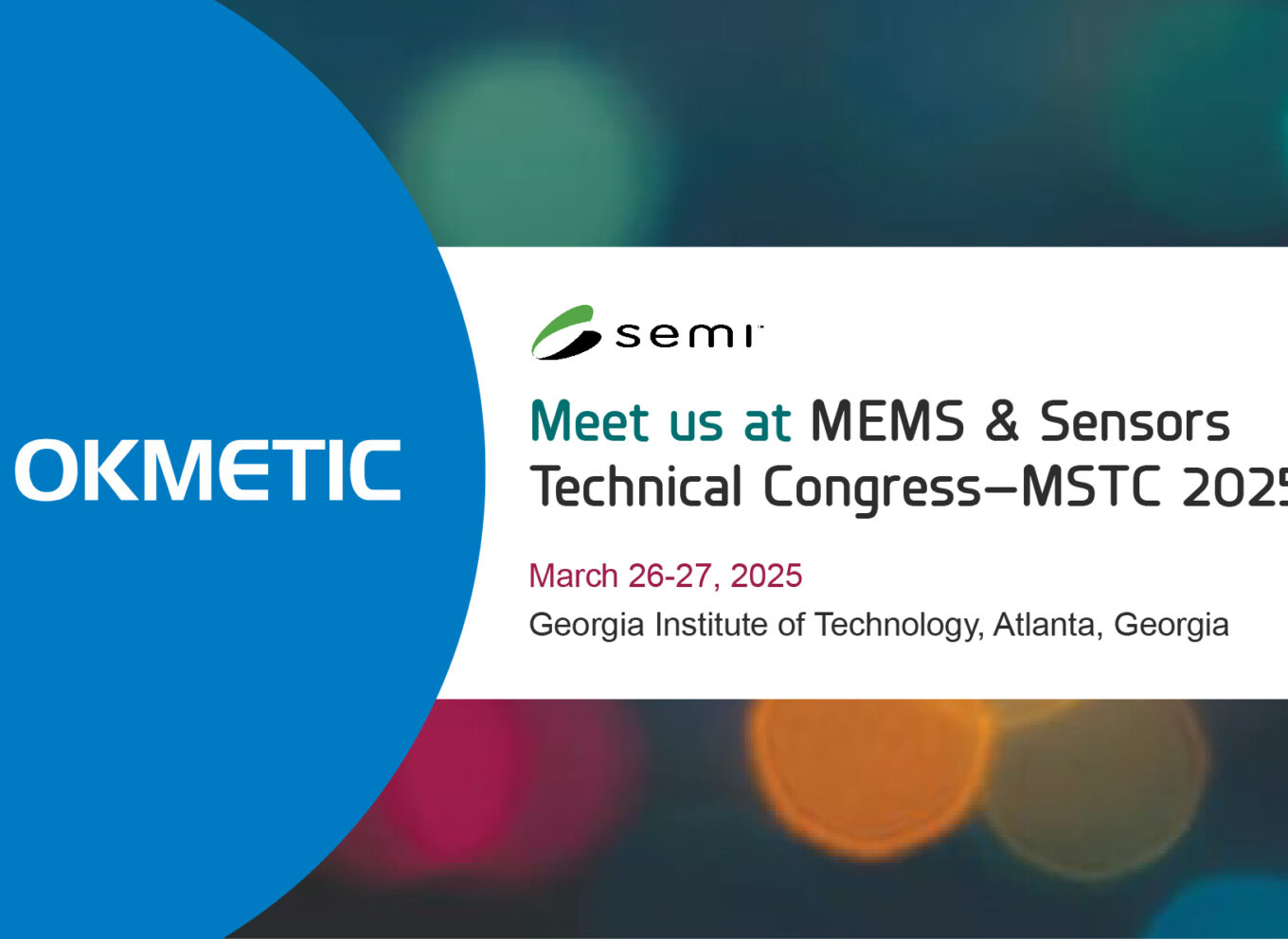
Okmetic is participating in MSTC
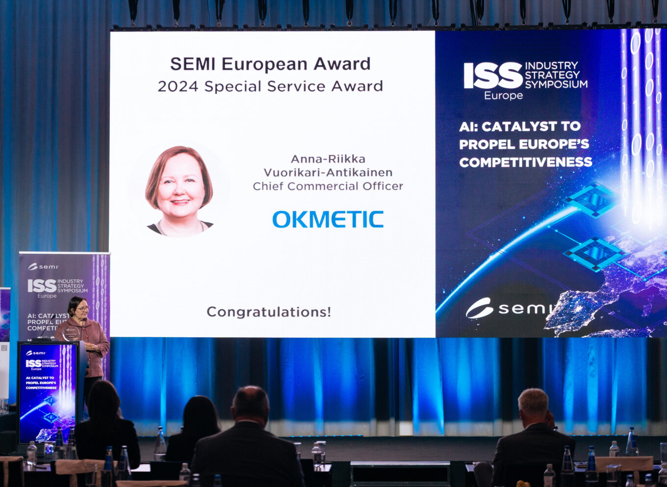
Okmetic CCO receives SEMI Europe Special Service Award
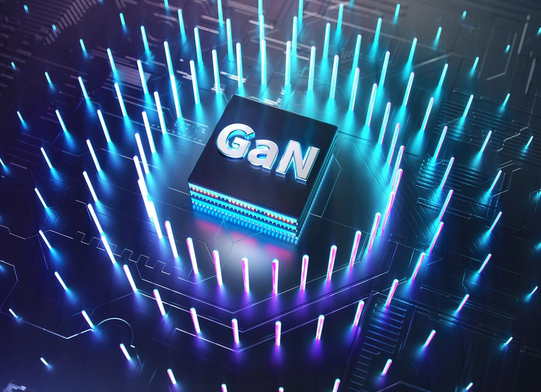
Power GaN Silicon and SOI Substrate wafers: Advancing high-performance GaN growth
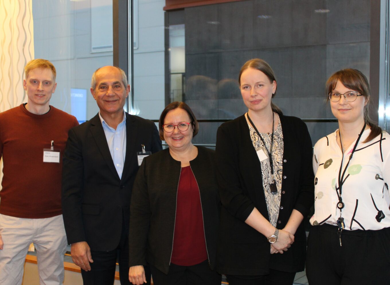
Okmetic welcomed SEMI Europe’s Laith Altimime to discuss European semiconductor industry
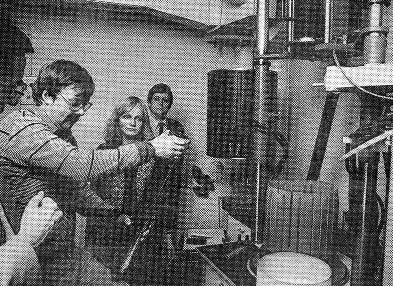
Pioneer in silicon crystals: Markku Tilli’s story
Okmetic is participating in SEMICON® Korea!