Events
Select content category

Okmetic participating in 20th Silicon Saxony Days

Okmetic participating in Semicon Connect

Okmetic participating in SEMICON Southeast Asia

R&D Director Heikki Holmberg speaking at Incize RF Workshop

Okmetic is participating in Applied Power Electronics Conference (APEC)

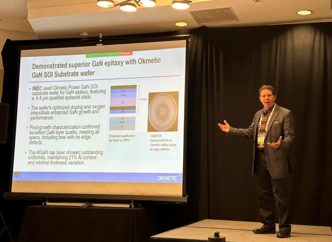
Jim Reed, President of Okmetic Inc. giving speech at Semicon West

Okmetic CTO Atte Haapalinna giving speech at the 2025 International RF-SOI Workshop

Okmetic participating in 2025 IC WORLD Conference
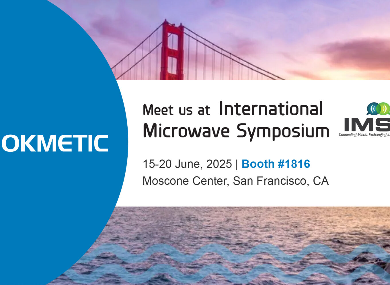
Okmetic participating in International Microwave Symposium
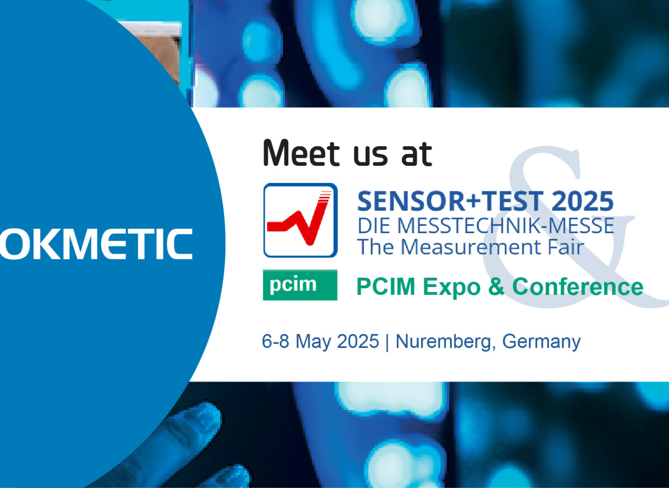
Okmetic attending PCIM Europe and SENSOR+TEST
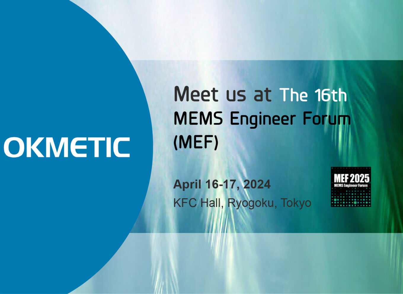
Okmetic participating in MEMS Engineer Forum
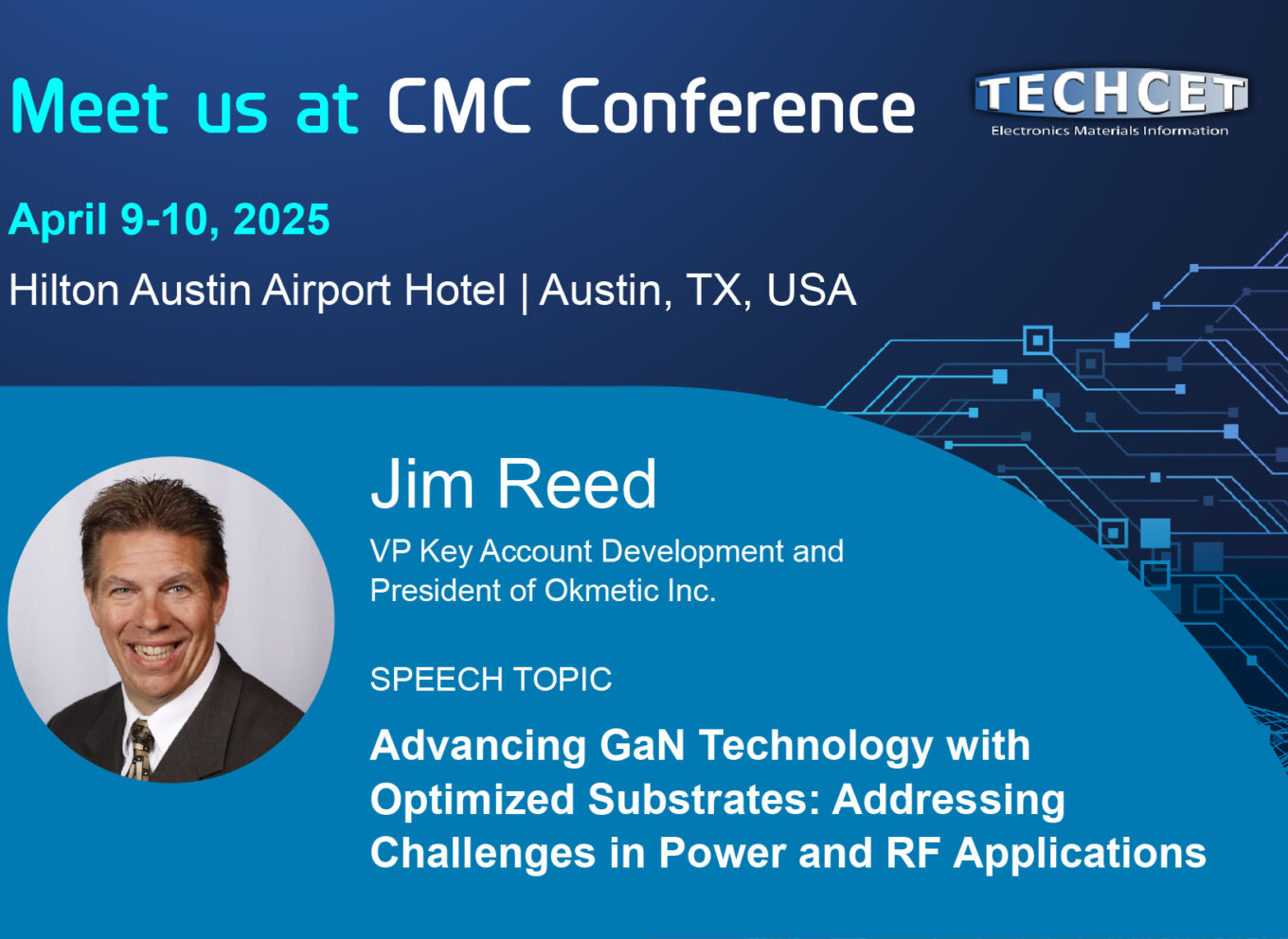
Okmetic Inc. President Reed gave a speech about substrates for GaN-on-Si and GaN-on-SOI at CMC Conference
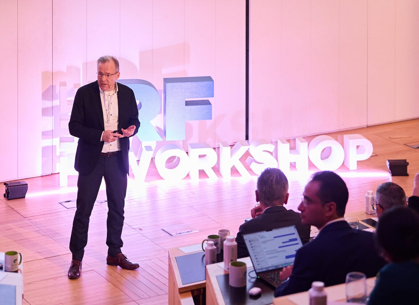
CTO Haapalinna gave a speech at Incize RF Workshop
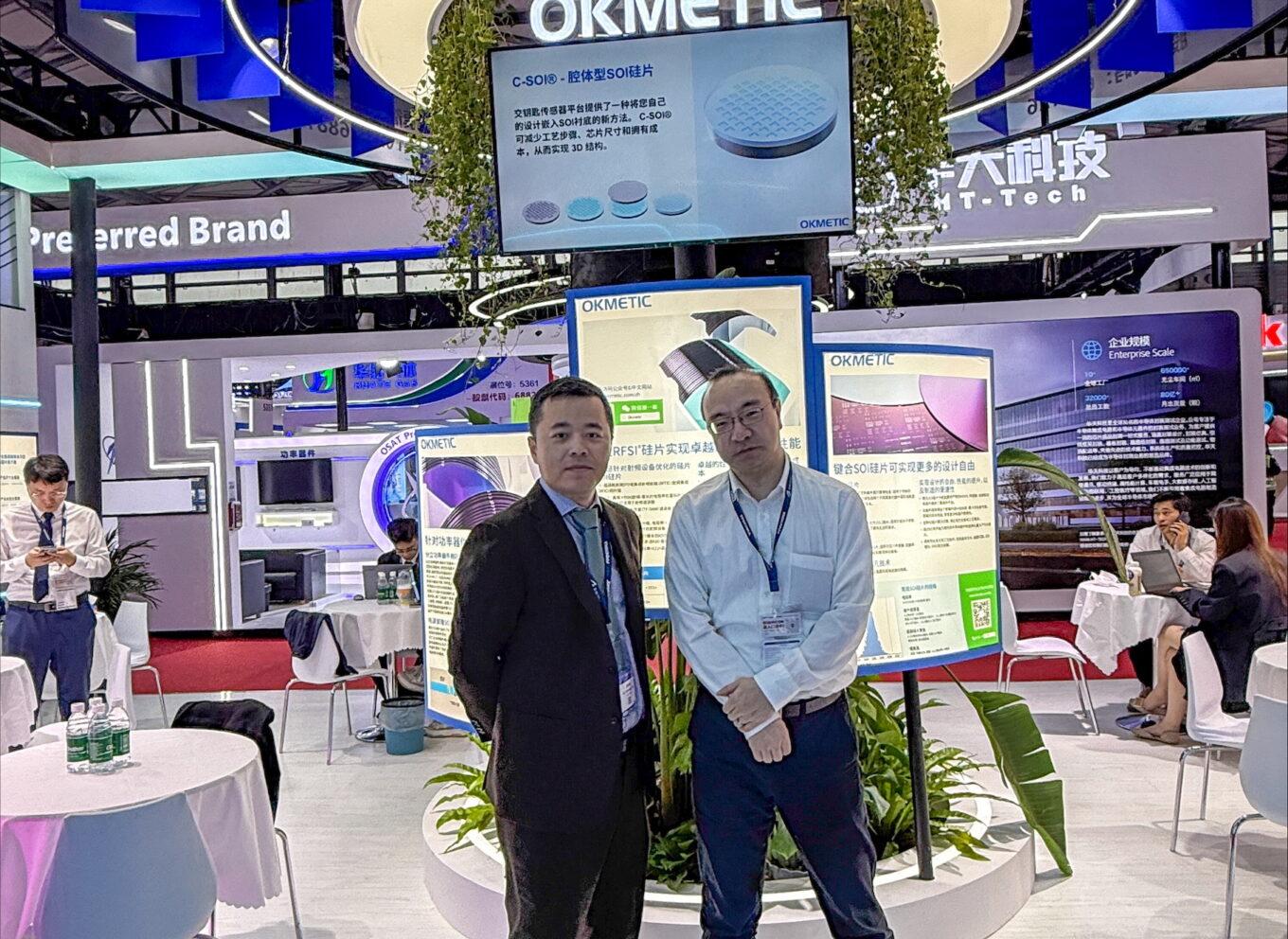
Okmetic participated in SEMICON China