Product news
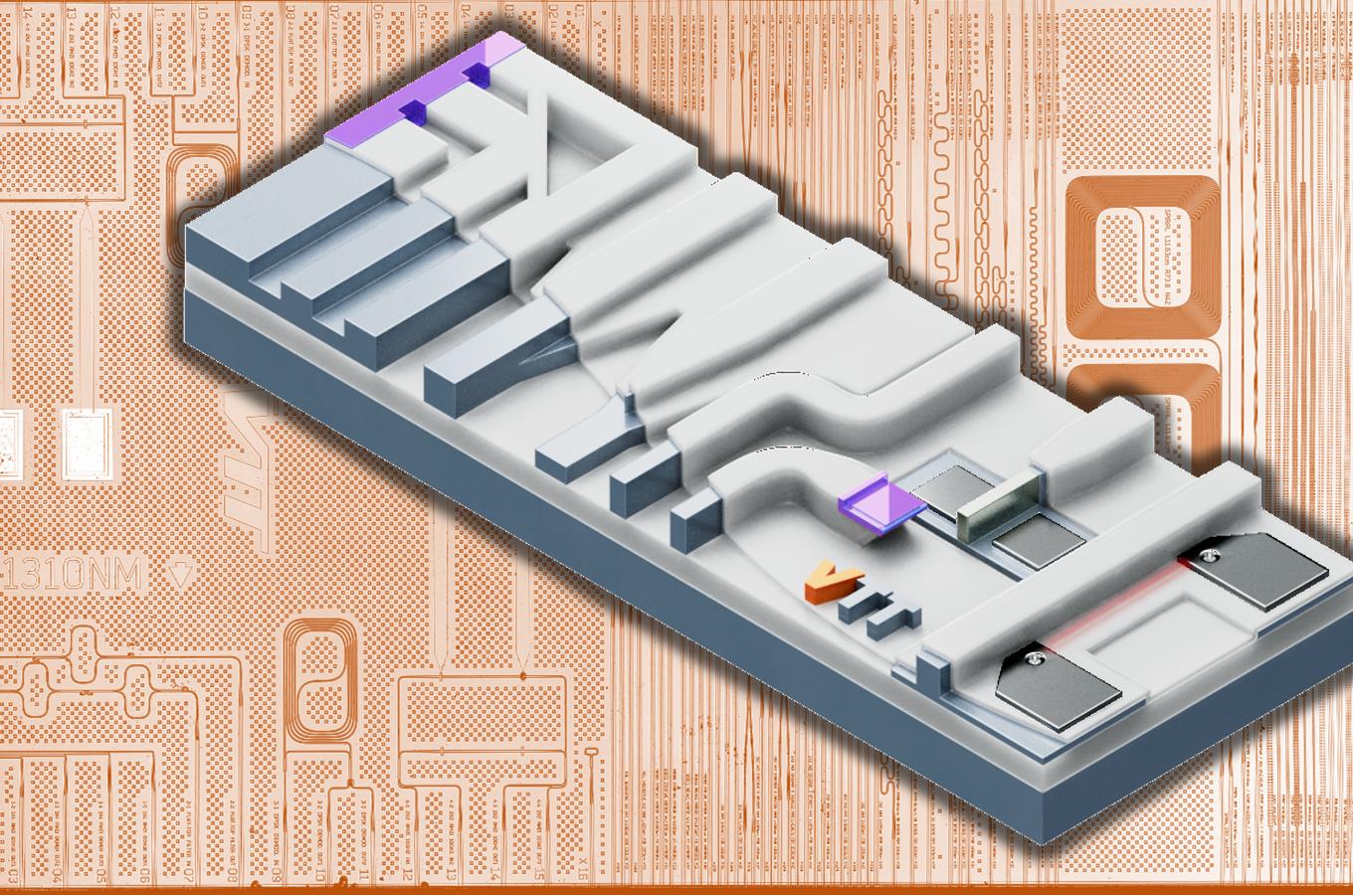
Select content category

Terrace Free SOI: maximizing usable wafer area

CCO Vuorikari-Antikainen: Okmetic expands wafer portfolio with 300 mm and epitaxial wafers to address broader customer requirements
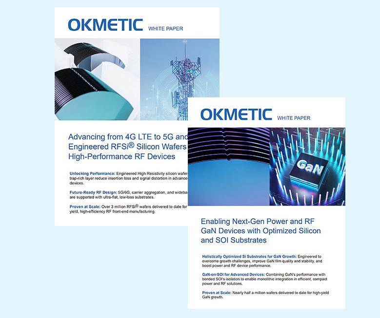
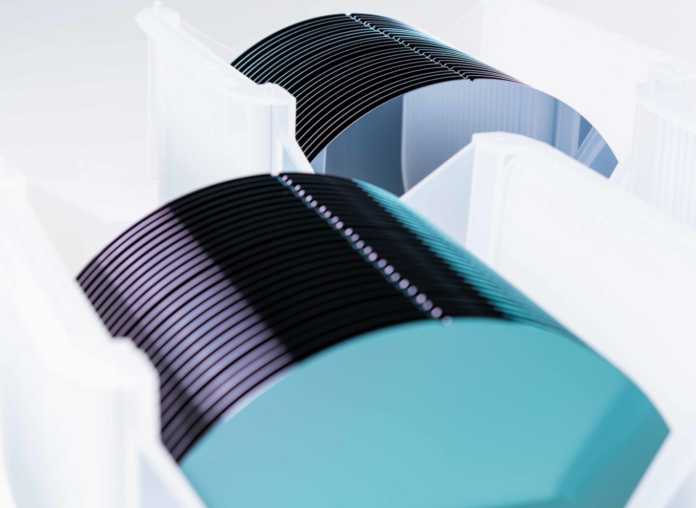
Two new whitepapers: Engineered Si wafers for RF devices and silicon/SOI substrates for GaN growth
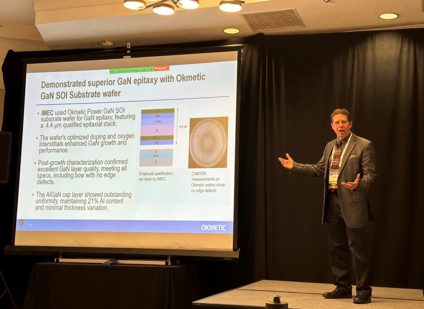
Okmetic Inc. President Reed gave a speech about substrates for GaN-on-Si and GaN-on-SOI at CMC Conference
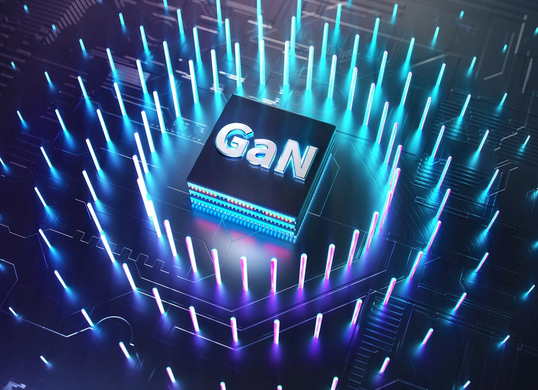
Power GaN Silicon and SOI Substrate wafers: Advancing high-performance GaN growth
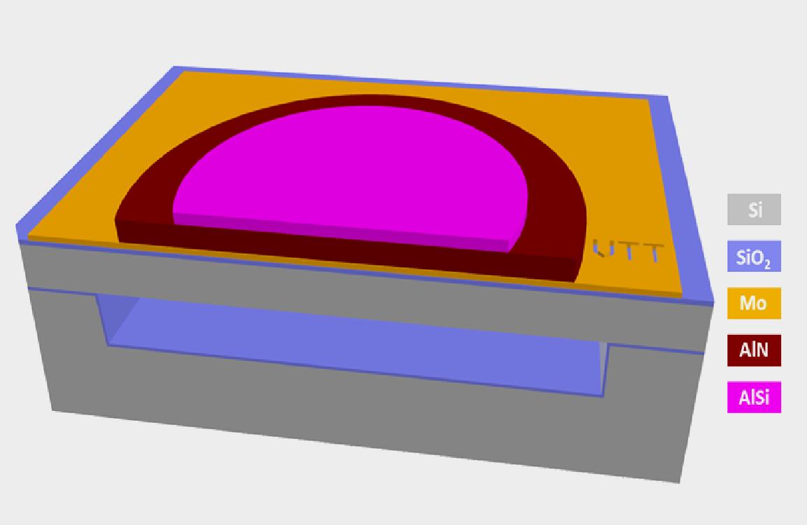
Enhancing PMUT performance with C-SOI® and EC-SOI wafers: Results from VTT – Okmetic collaboration

Okmetic participating in projects bridging the RF frequency gap
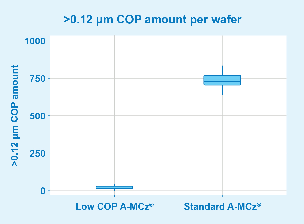
COP level management enhancing power device reliability and yield
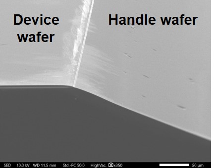
Okmetic launches Terrace Free SOI capability
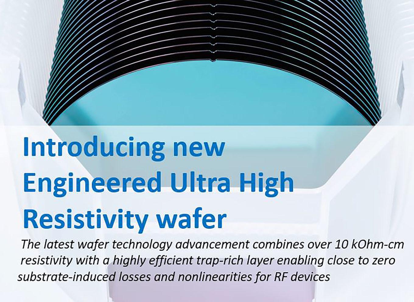
Okmetic Expands Its RFSi® Portfolio with Engineered Ultra High Resistivity Wafer
VTT finds Okmetic E-SOI® wafers highly beneficial platform for its Photonics Technology