News & insights
Select content category
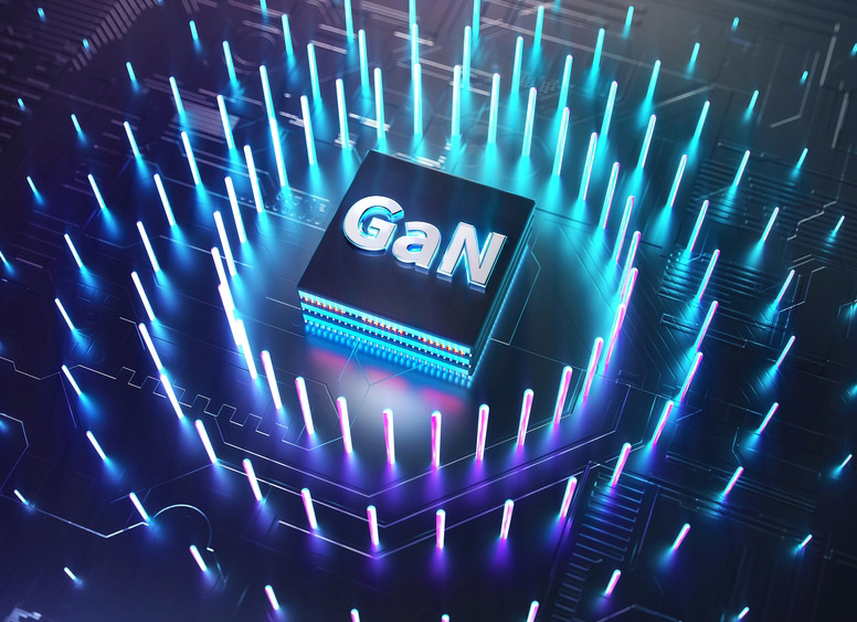
Power GaN Silicon and SOI Substrate wafers: Advancing high-performance GaN growth
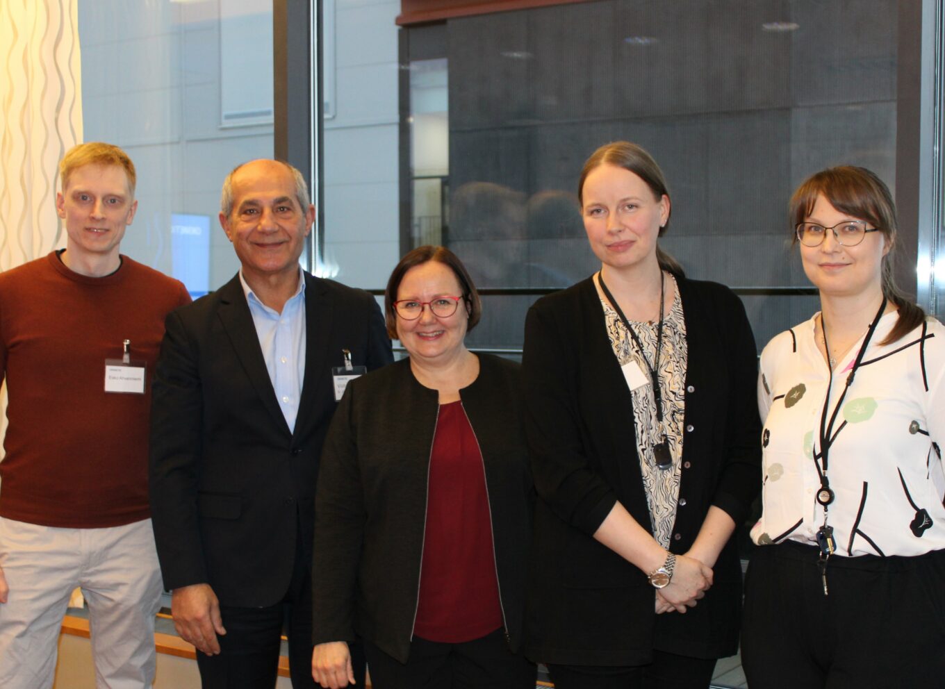
Okmetic welcomed SEMI Europe’s Laith Altimime to discuss European semiconductor industry
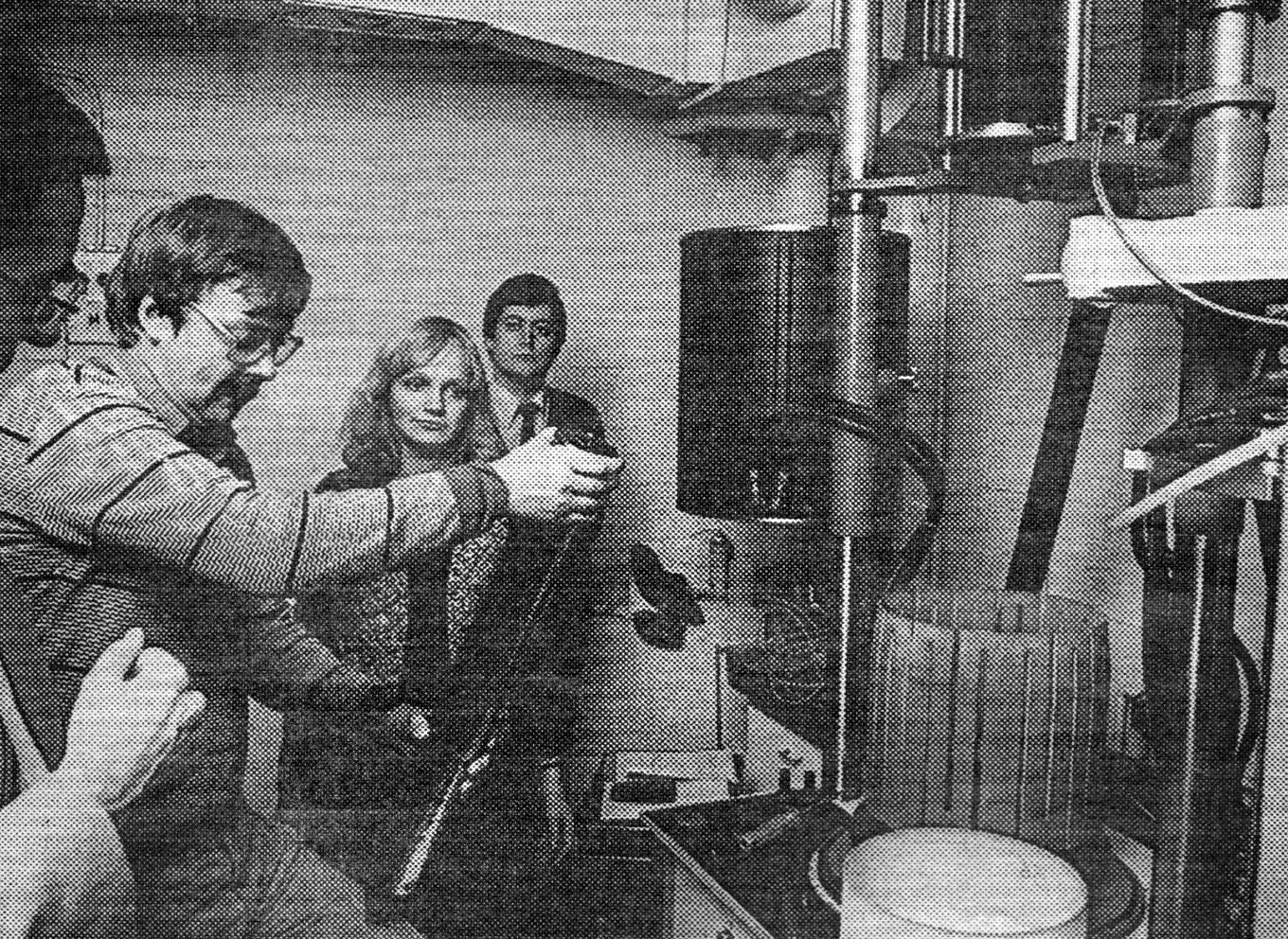
Pioneer in silicon crystals: Markku Tilli’s story
Okmetic is participating in SEMICON® Korea!
Okmetic participating SPIE Photonics West
CEO Kai Seikku: Moving Forward Together with Semiconductor Market Recovery on the Horizon
Silicon pioneer Veikko Lindroos made Okmetic’s story possible
Season’s Greetings from Okmetic
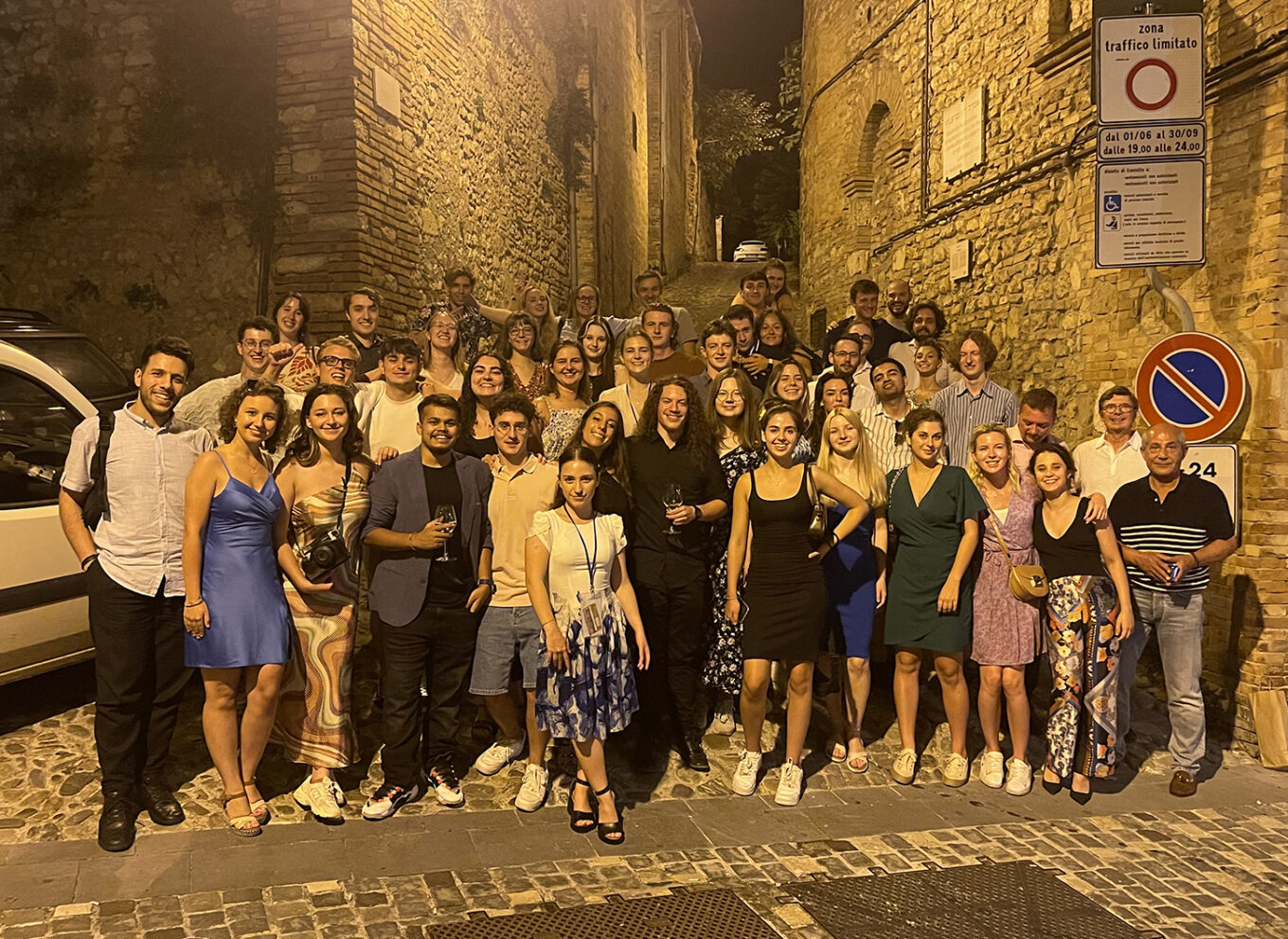
ECS Summer School 2024 brought students comprehensive knowledge of semiconductor industry
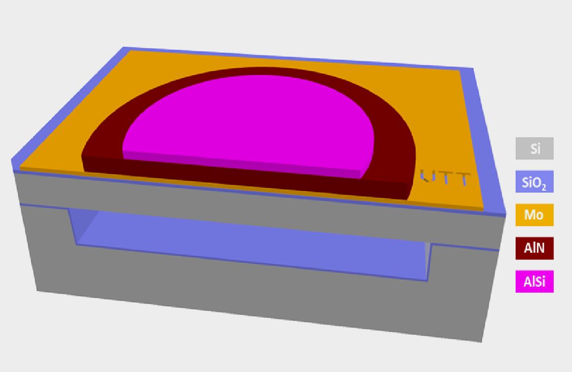
Enhancing PMUT performance with C-SOI® and EC-SOI wafers: Results from VTT – Okmetic collaboration
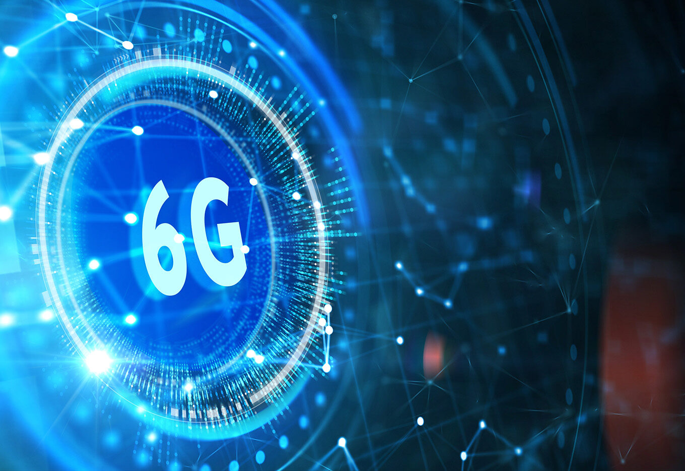
Okmetic participating in projects bridging the RF frequency gap
Okmetic participating in CMC Seminar 23 October
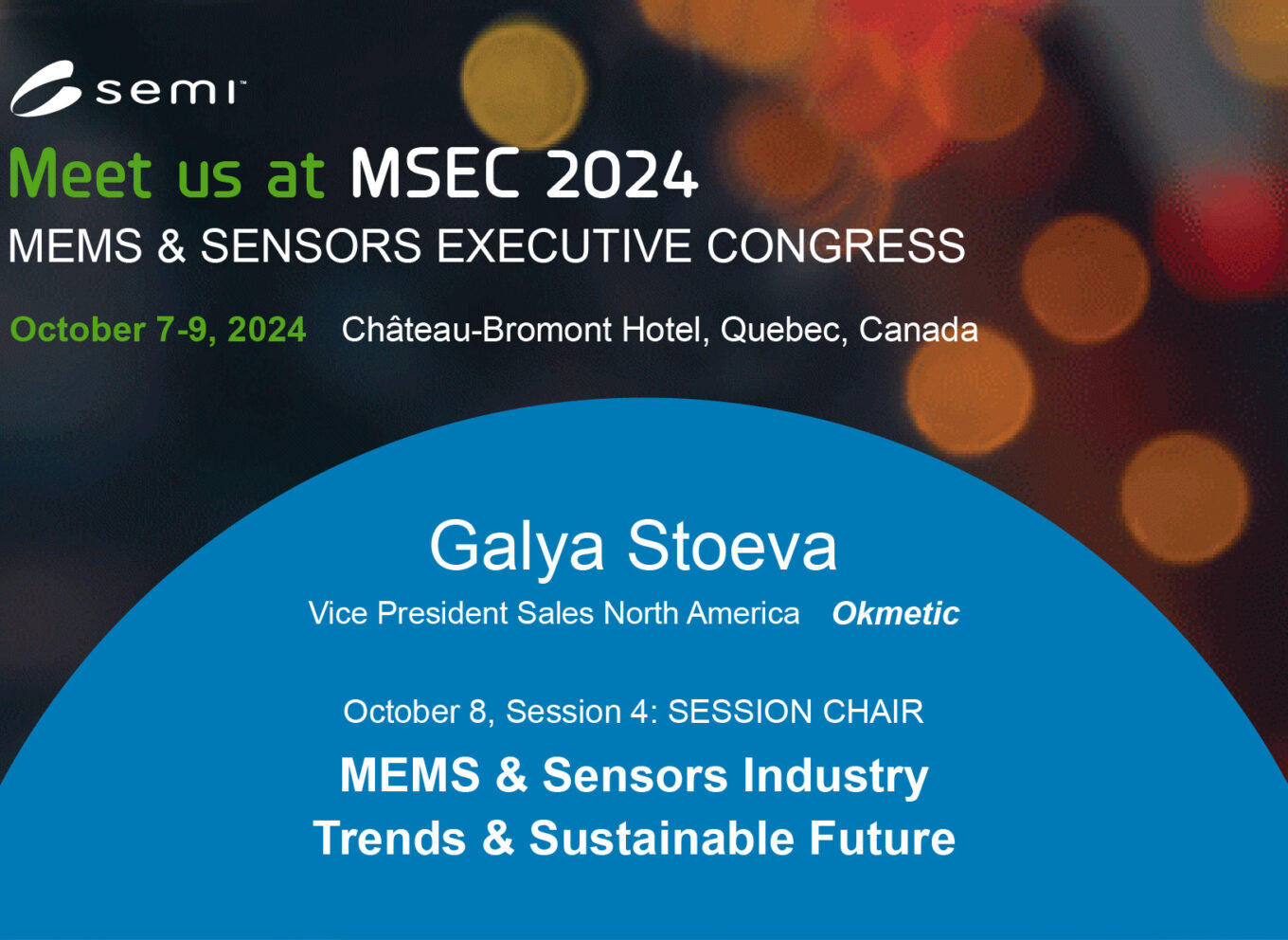
Okmetic is participating in MSEC