News & insights
Select content category

CEO Kai Seikku: Moving Forward Together with Semiconductor Market Recovery on the Horizon
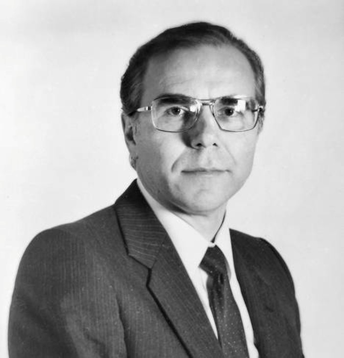
Silicon pioneer Veikko Lindroos made Okmetic’s story possible
Season’s Greetings from Okmetic
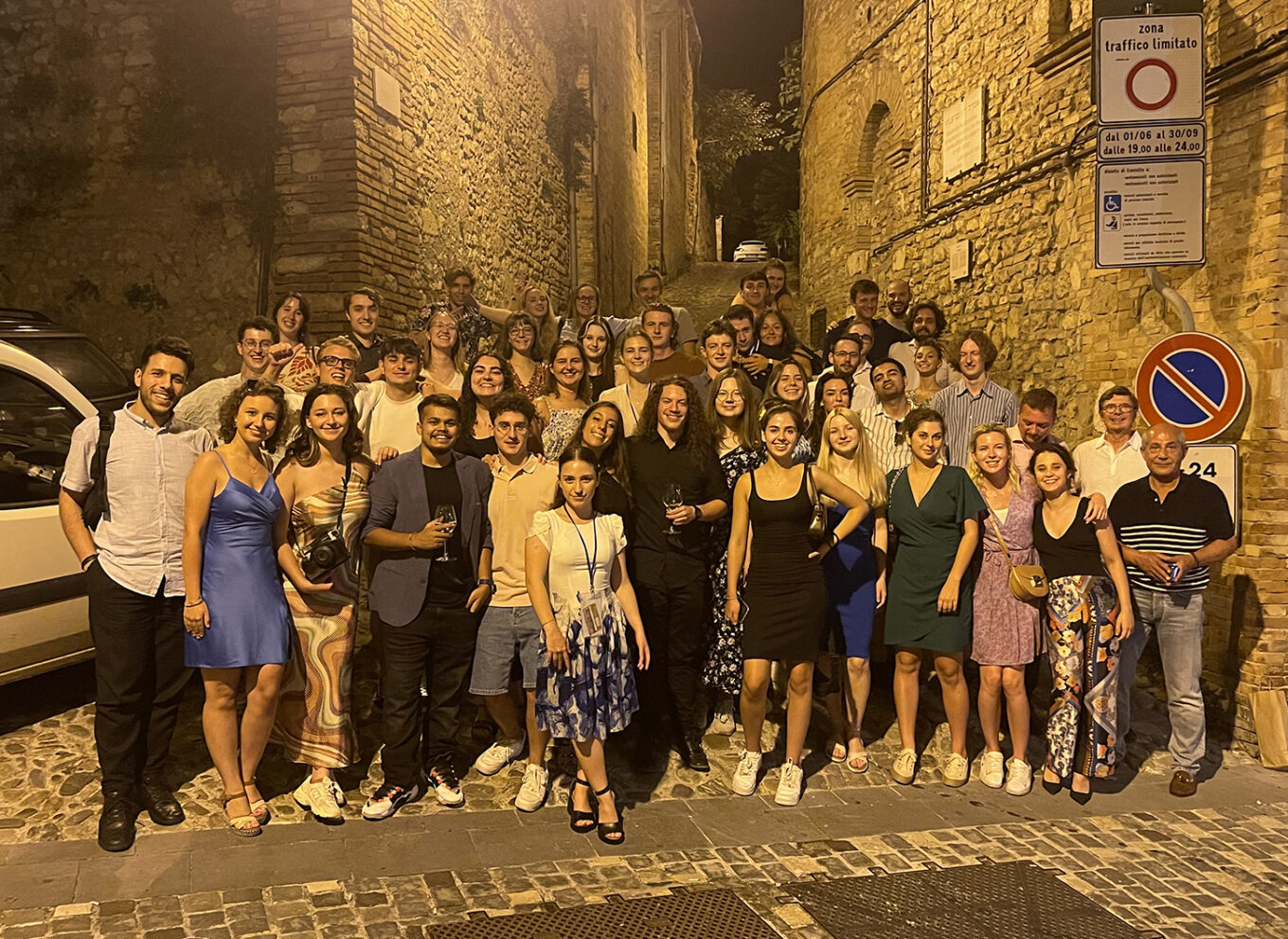
ECS Summer School 2024 brought students comprehensive knowledge of semiconductor industry
Enhancing PMUT performance with C-SOI® and EC-SOI wafers: Results from VTT – Okmetic collaboration

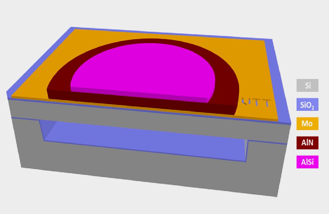
Okmetic participating in projects bridging the RF frequency gap
Okmetic participating in CMC Seminar 23 October
Okmetic is participating in MSEC
Okmetic will be participating in ISES US Power
Okmetic participates in the ECSA project to respond to the shortage of semiconductor professionals
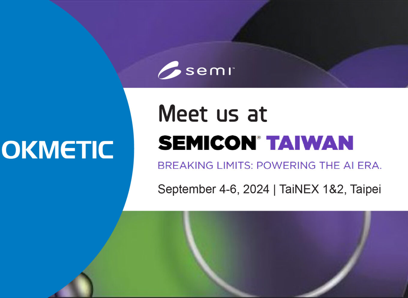
Okmetic is participating in SEMICON Taiwan
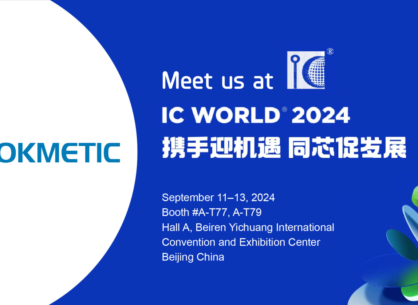
Okmetic participating Beijing Microelectronics International Symposium
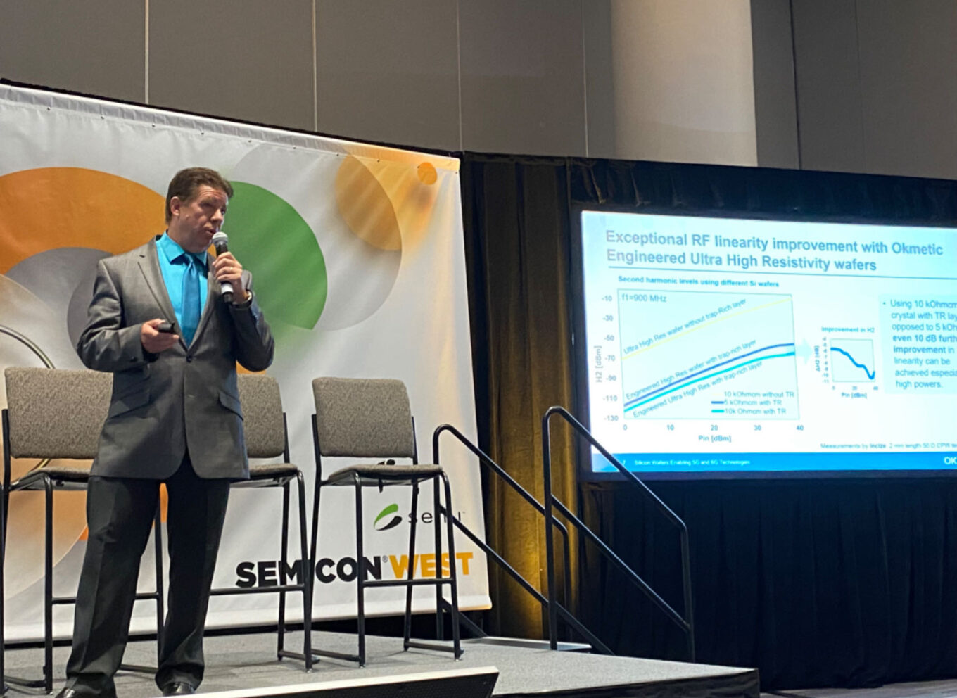
Jim Reed held a speech at Semicon West 2024
Okmetic commits to Science Based Targets Initiative (SBTi) to strengthen its sustainability work