News & insights
Select content category
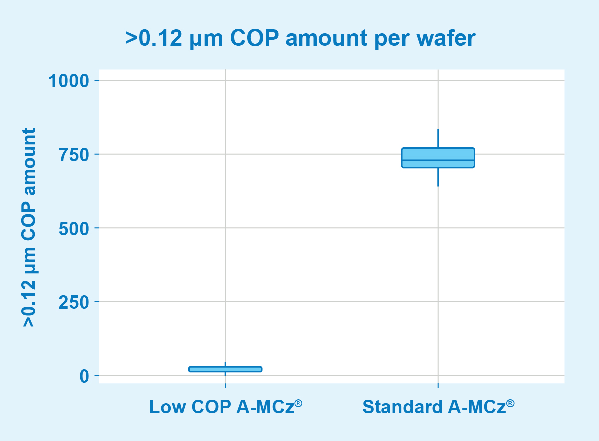
COP level management enhancing power device reliability and yield
New strategy outlines growth opportunities for Finnish semiconductor industry
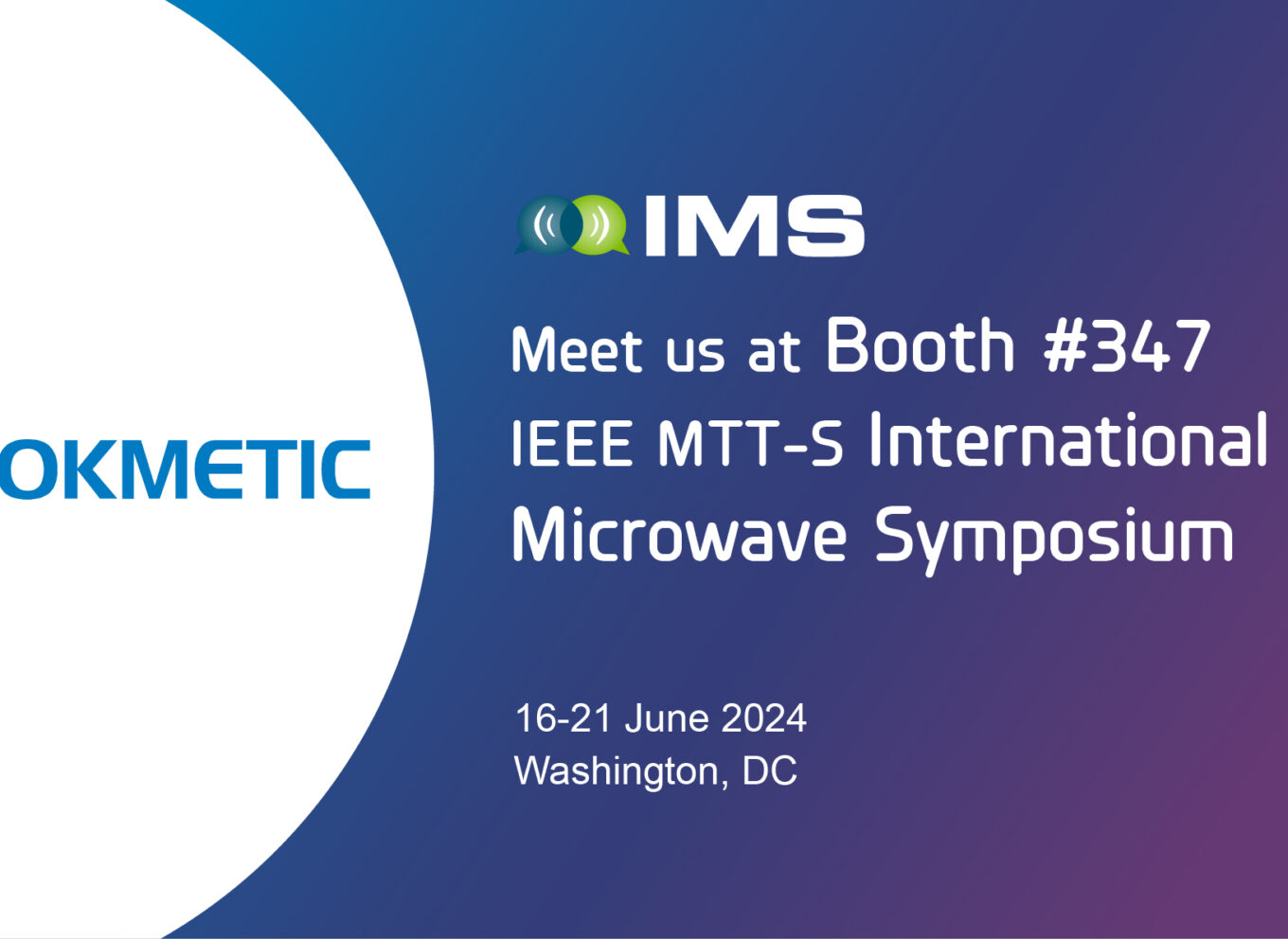
Join Okmetic at IMS2024 on 16-21 June 2024, in Washington, DC
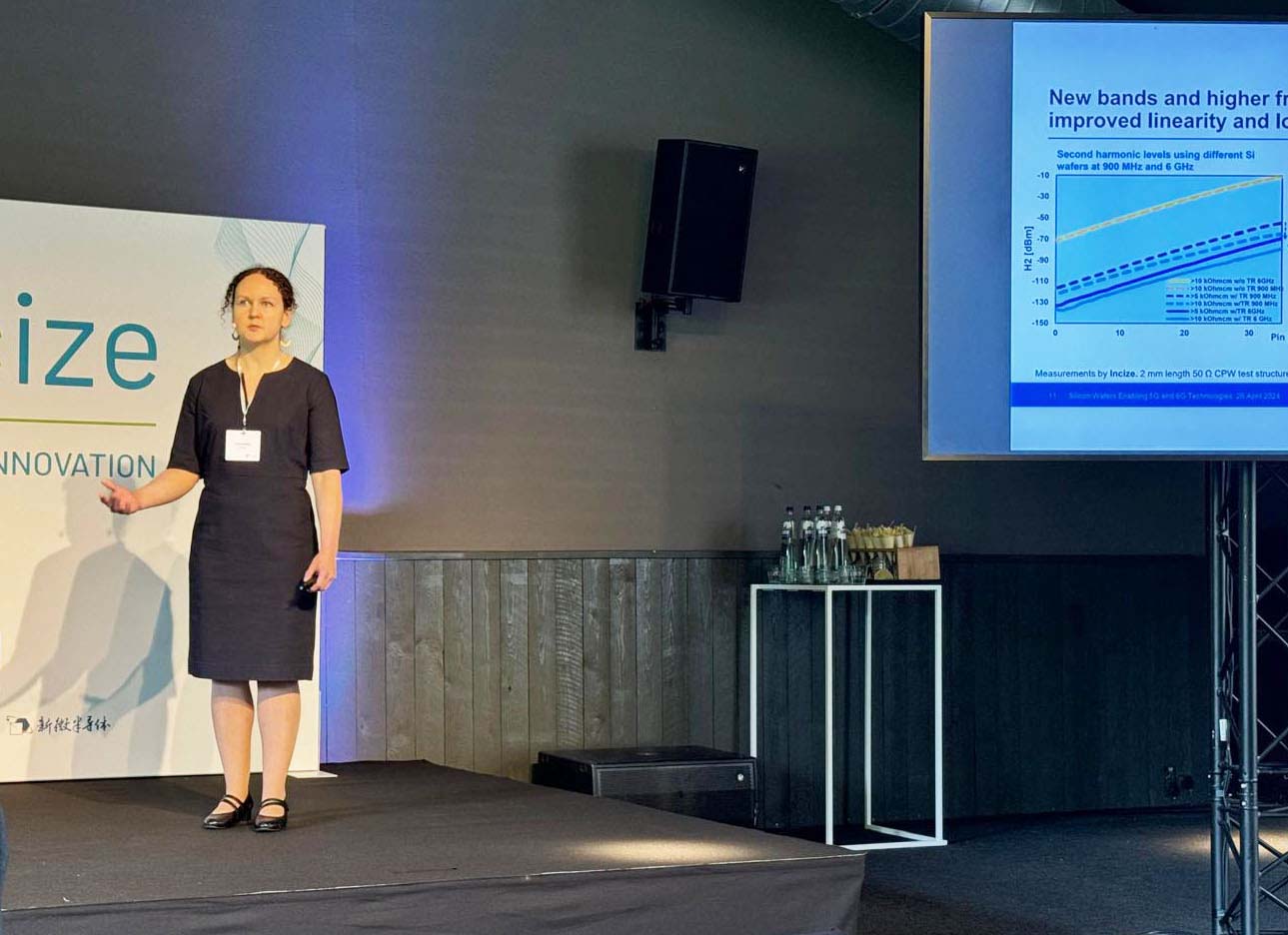
Katja Parkkinen held a speech at Incize RF Workshop
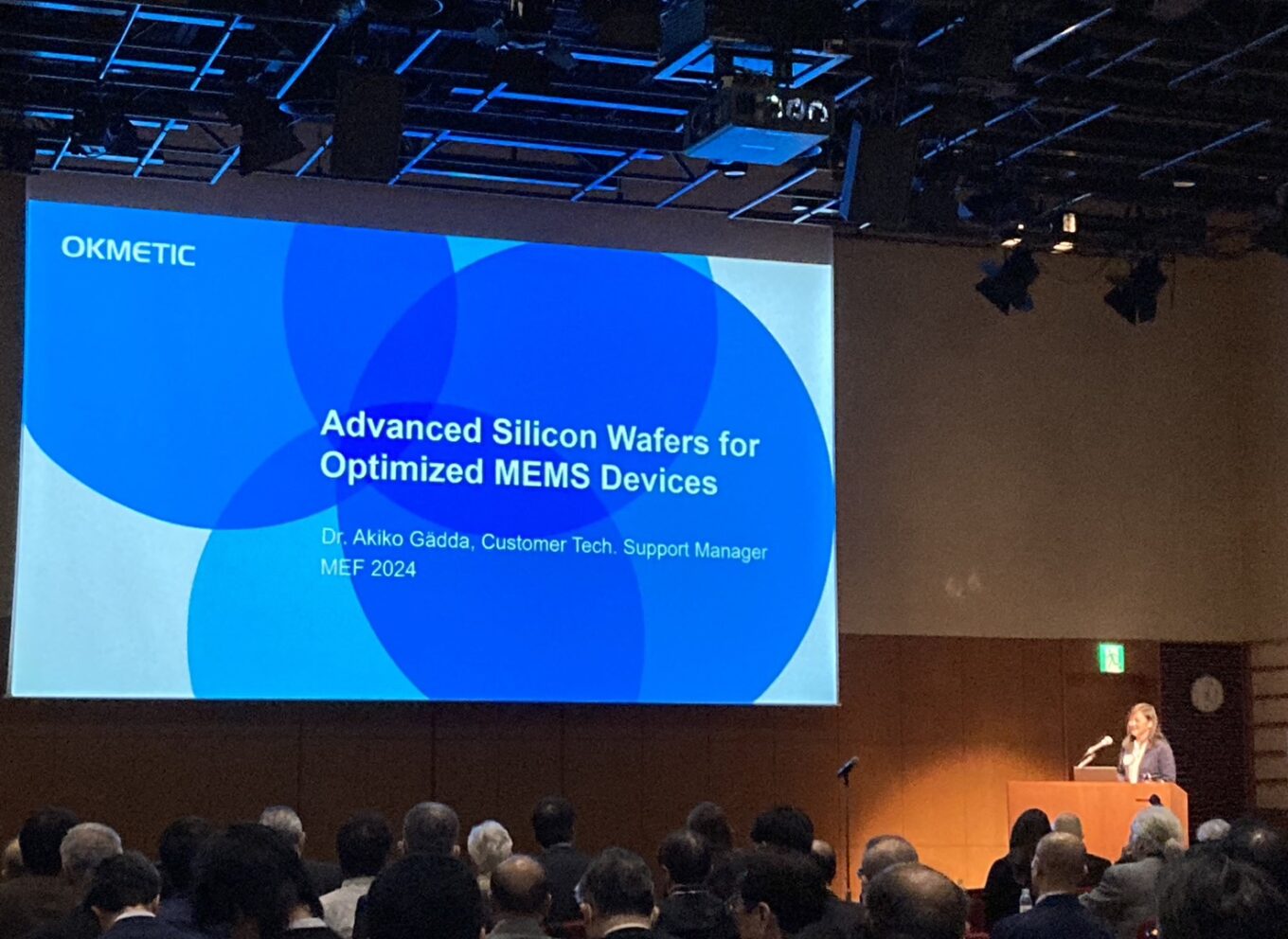
Dr. Akiko Gädda gave a speech at the MEF
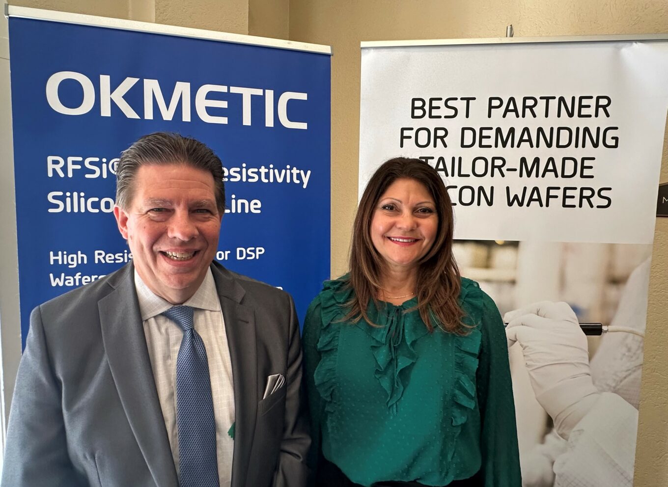
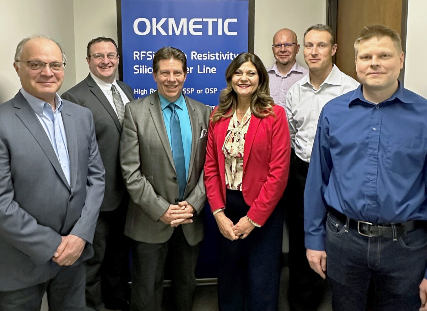
Okmetic participated in CMC Techcet event
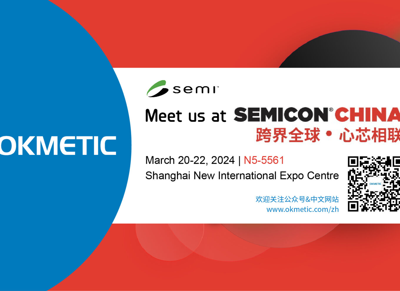
Okmetic is participating in the SEMICON China 2024 during March 20-22 in Shanghai
Okmetic Inc. has achieved a 25 year milestone
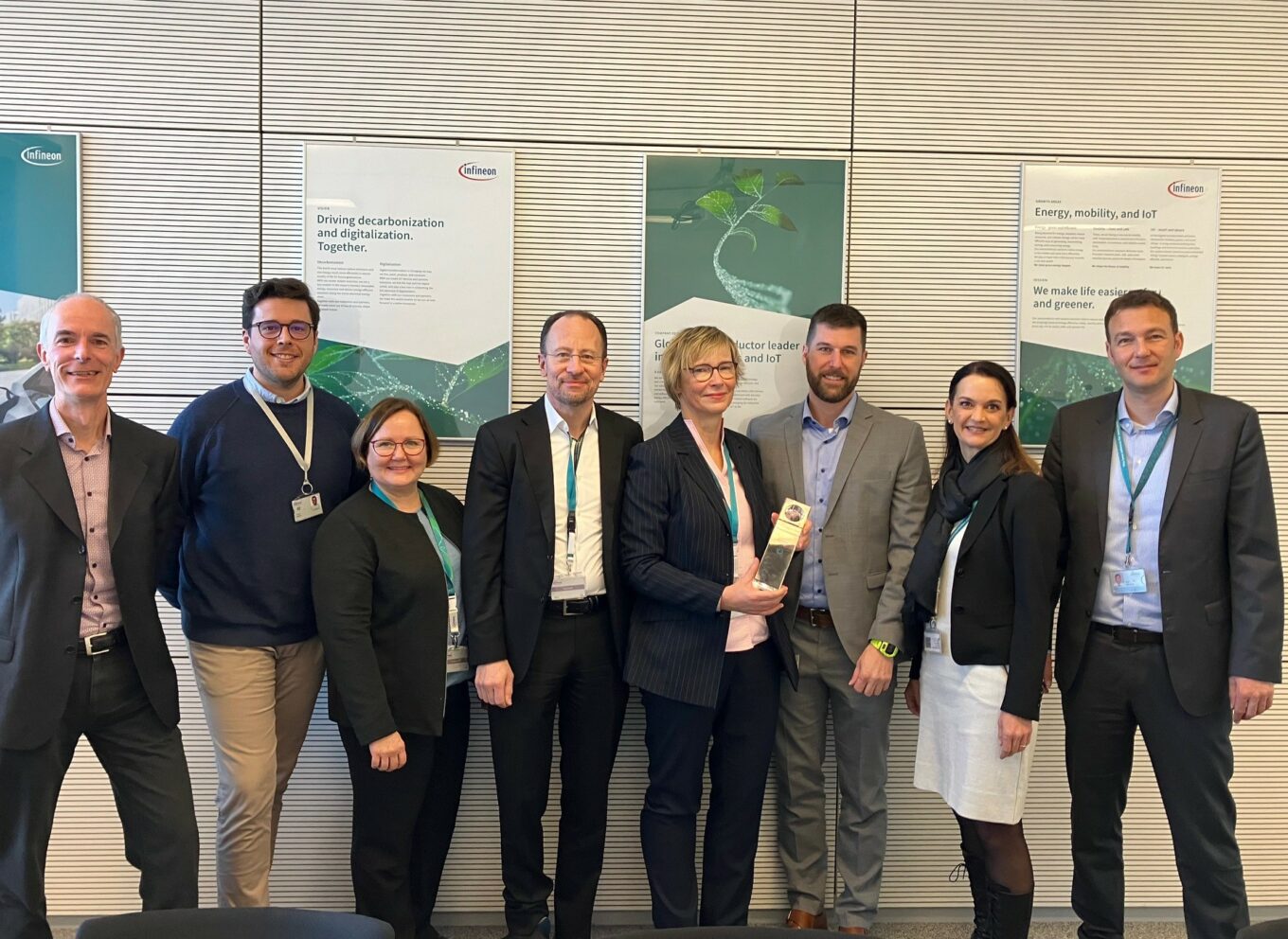
Okmetic receives Infineon’s Best Wafer Supplier award 2023
Okmetic recertified to conform to IATF 16949:2016 standards
Happy Lunar New Year 2024
Okmetic is participating in the MEMS Sensing and Network System in Tokyo
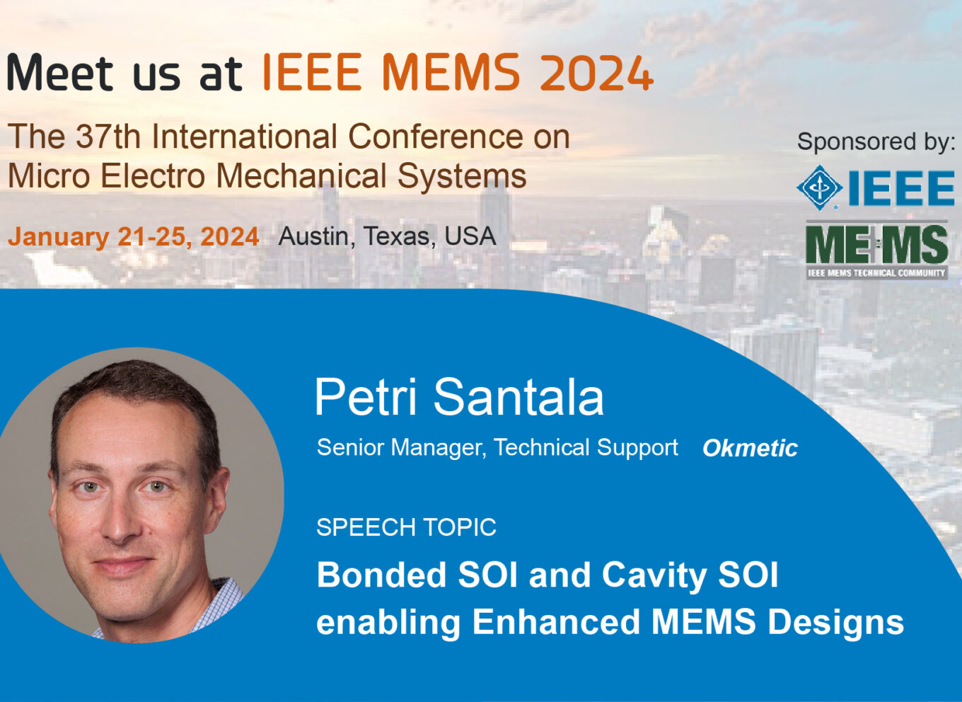
Okmetic is participating in the IEEE MEMS Conference 2024, to be held in Austin, Texas
Okmetic is participating SEMICON® KOREA from January 31-February 2