News & insights
Select content category
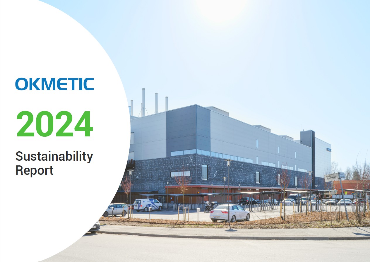
The Sustainability Report for 2024 has been published
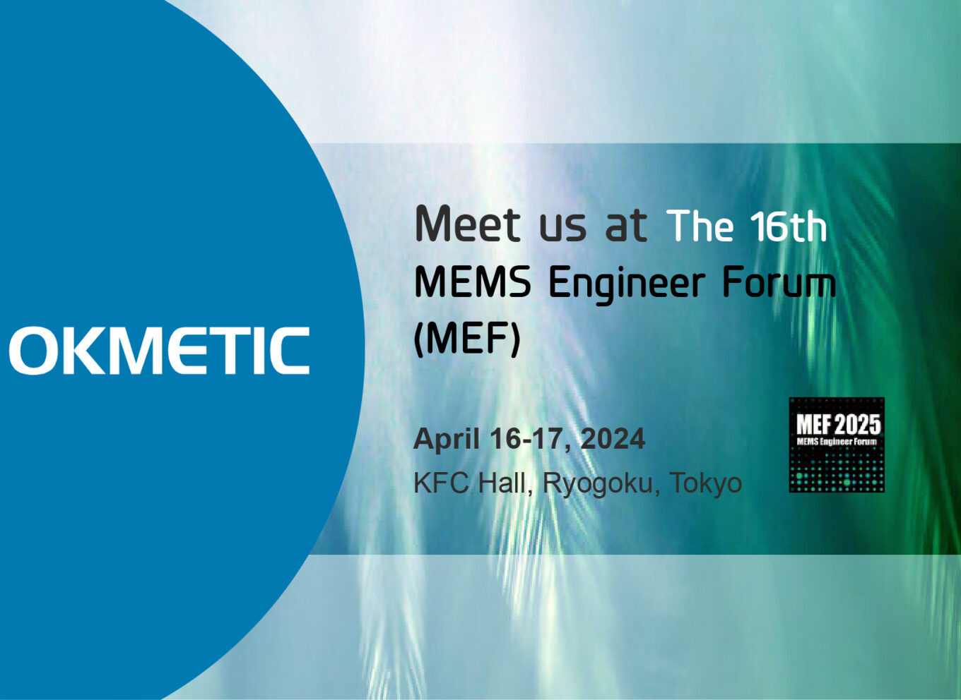
Okmetic participating in MEMS Engineer Forum
Okmetic achieved the highest Platinum level in a sustainability audit
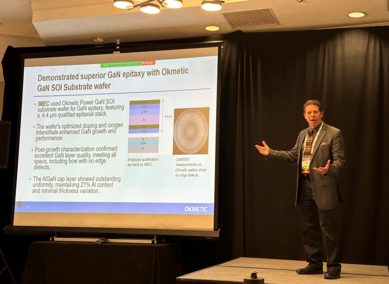
Okmetic Inc. President Reed gave a speech about substrates for GaN-on-Si and GaN-on-SOI at CMC Conference
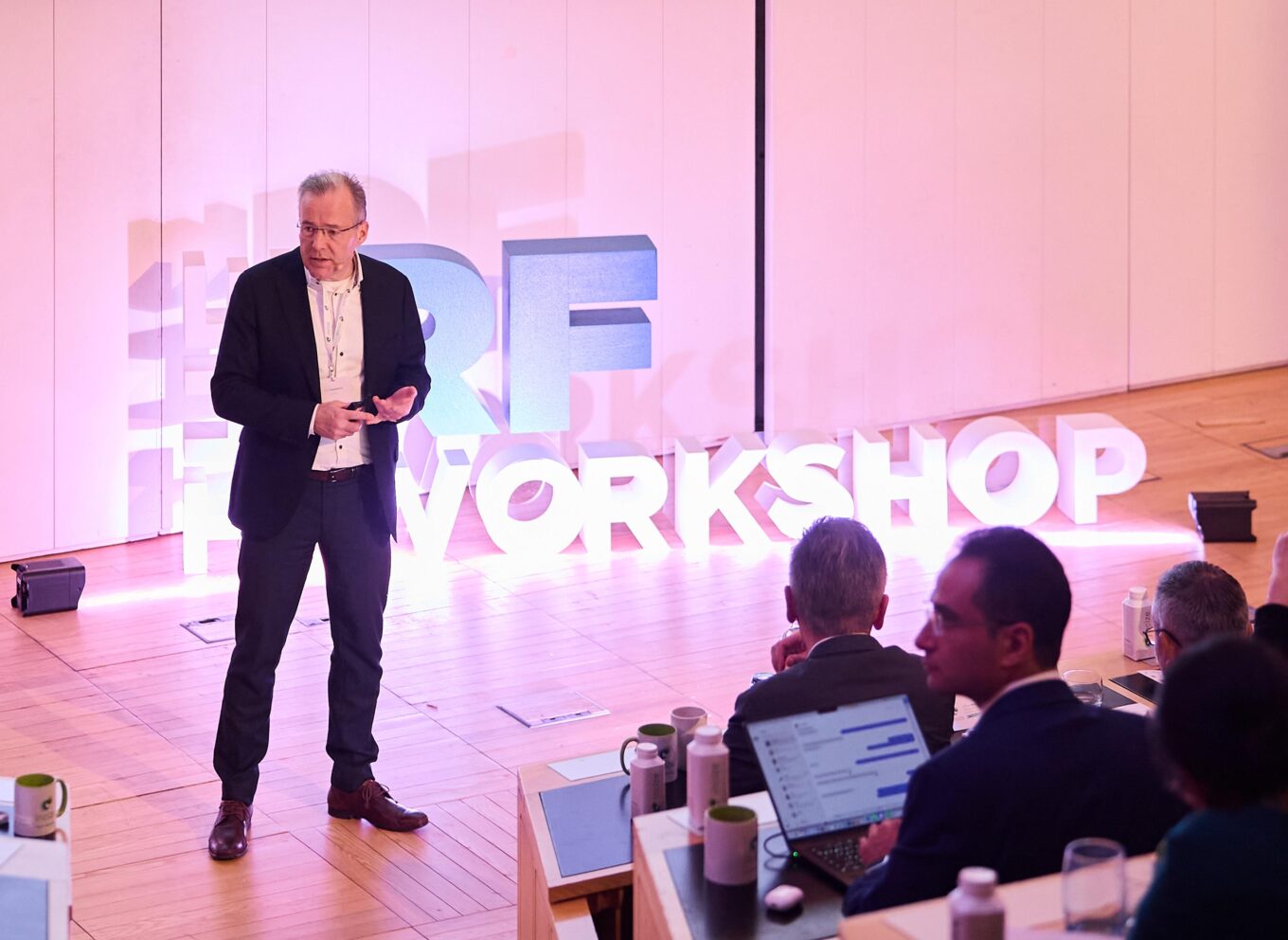
CTO Haapalinna gave a speech at Incize RF Workshop
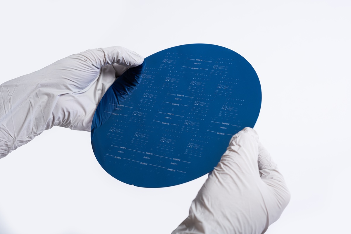
20 years of C-SOI®: Enabling streamlined production of high-performance MEMS devices
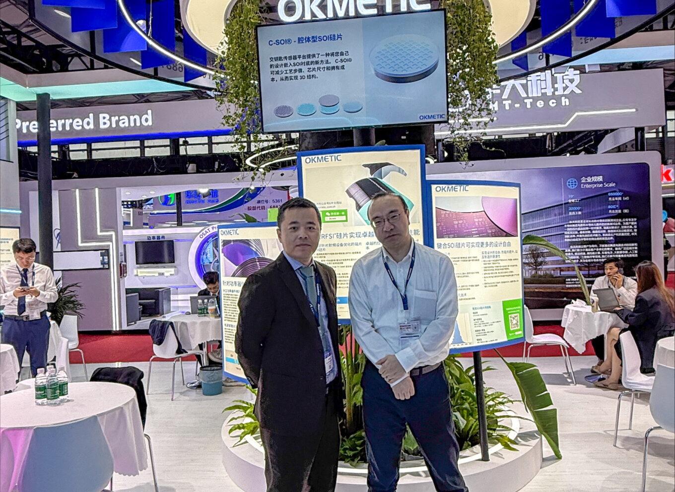
Okmetic participated in SEMICON China

Okmetic Inc. President Jim Reed giving a speech at CMC Conference
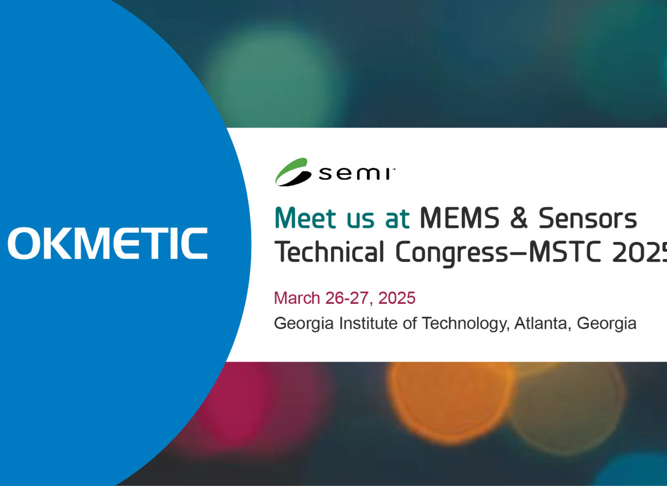
Okmetic is participating in MSTC
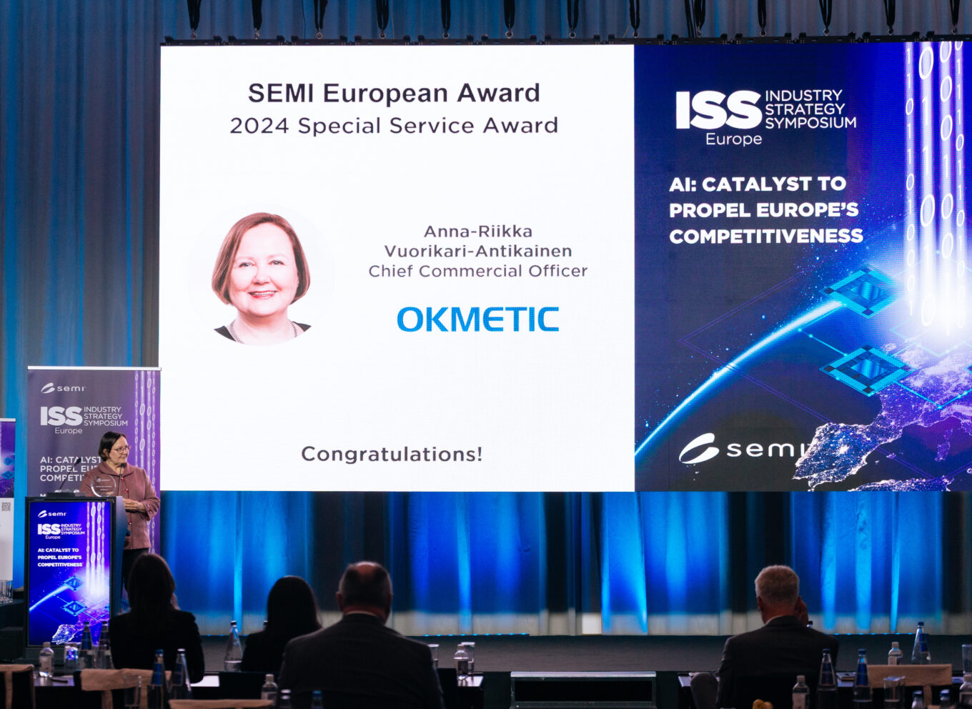
Okmetic CCO receives SEMI Europe Special Service Award
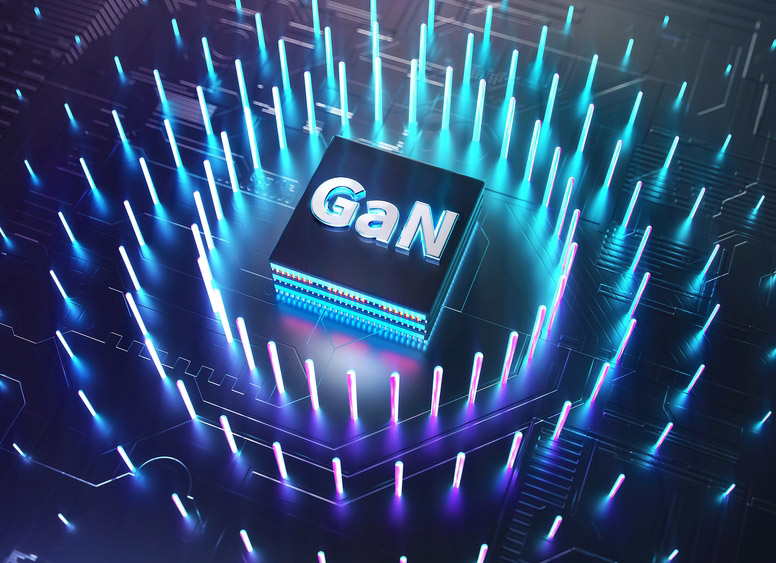
Power GaN Silicon and SOI Substrate wafers: Advancing high-performance GaN growth
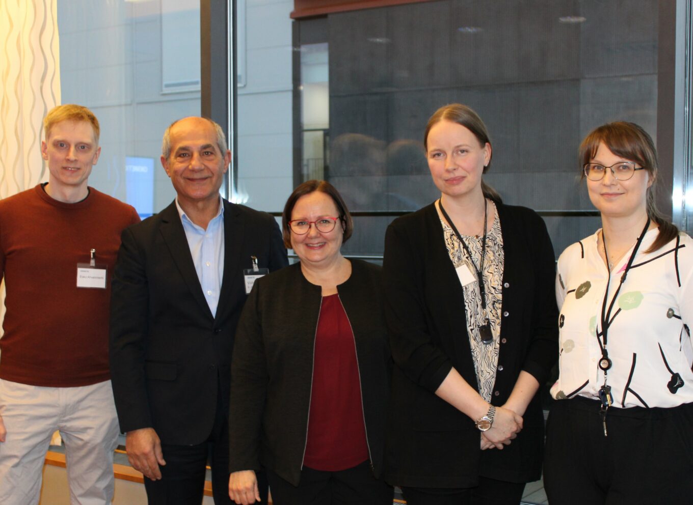
Okmetic welcomed SEMI Europe’s Laith Altimime to discuss European semiconductor industry
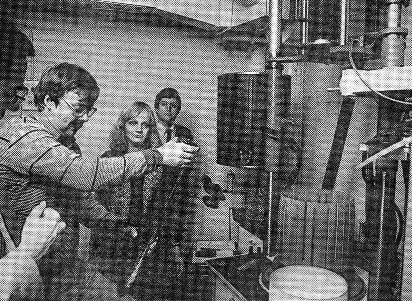
Pioneer in silicon crystals: Markku Tilli’s story
Okmetic is participating in SEMICON® Korea!