Skip to content
To front page
  • Silicon Wafers 150-200 mm
    • MEMS Wafer Line
      • MEMS SSP and DSP Wafers
      • Selecting the ideal wafer for MEMS devices: Balancing cost, performance, and manufacturing efficiency
    • RFSi® Wafer Line – High Resistivity for RF
      • High Resistivity Wafers
      • Engineered High Resistivity Wafers with Trap-Rich Layer
      • Engineered Ultra High Resistivity wafers
      • UF-RFSi® – Ultra Flat High Resistivity Wafers
      • High Resistivity BSOI Wafers
      • RF GaN Substrate wafers
      • White paper “Advancing from 4G LTE to 5G and 6G: Engineered RFSi® Silicon Wafers for High-Performance RF Devices”
    • Power Wafer Line
      • Power Management SOI wafers
      • Power GaN Substrate wafers (Si and SOI) 
      • Discrete Power Device wafers 
      • White paper: “Enabling next-gen power and RF GaN devices with optimized silicon and SOI substrates” 
    • SOI Wafers – Silicon-On-Insulator Line
      • BSOI Wafers – Bonded SOI
      • C-SOI® Wafers – Cavity SOI
      • E-SOI® Wafers – Enhanced SOI
      • Terrace Free SOI Wafers
    • Patterned Wafers – DRIE and Lithography
    • TSV Wafers – Through Silicon Via
    • DSP Wafers – Double Side Polished
    • SSP Wafers – Single Side Polished
    • EPI Wafers – Epitaxial Silicon Wafers
    • Customized Wafers and Prototyping
    • Production and Capacity Expansion 
    • Supplier Awards and Collaboration Projects
  • Silicon wafers 300 mm
    • Polished silicon wafers 
    • Epitaxial (EPI) silicon wafers 
    • Test and monitor silicon wafers 
  • Applications
    • MEMS and Sensors
    • RF Filters and Devices
    • Power Devices
  • Quality
    • Certificates
    • Quality Policy
    • Quality Tools
      • Artificial Intelligence at Okmetic
      • 5S at Okmetic
  • Sustainability
    • Sustainability Report and Certificates
    • Environment and Targets
    • Responsibility for Personnel
    • Responsibility for Health and Safety
    • Business Ethics
    • Managing Responsibility
  • Work with Us
    • Production Experts
    • Semiconductor Professionals
    • Students
    • Maintenance professional
    • Technical professionals
    • Sales and technical support
    • Open Positions
  • About Okmetic
    • Company
    • Strategy and Values
    • Executive Management Group
    • Investments
    • Research and Development Work
    • Tale of a Silicon Wafer
    • The History of Okmetic
    • News & Insights
    • Contact Us
  • English
    • Suomi
    • 日本語
    • 中文 (中国)

Events

Okmetic+About Okmetic+News & insights+Events

Select content category
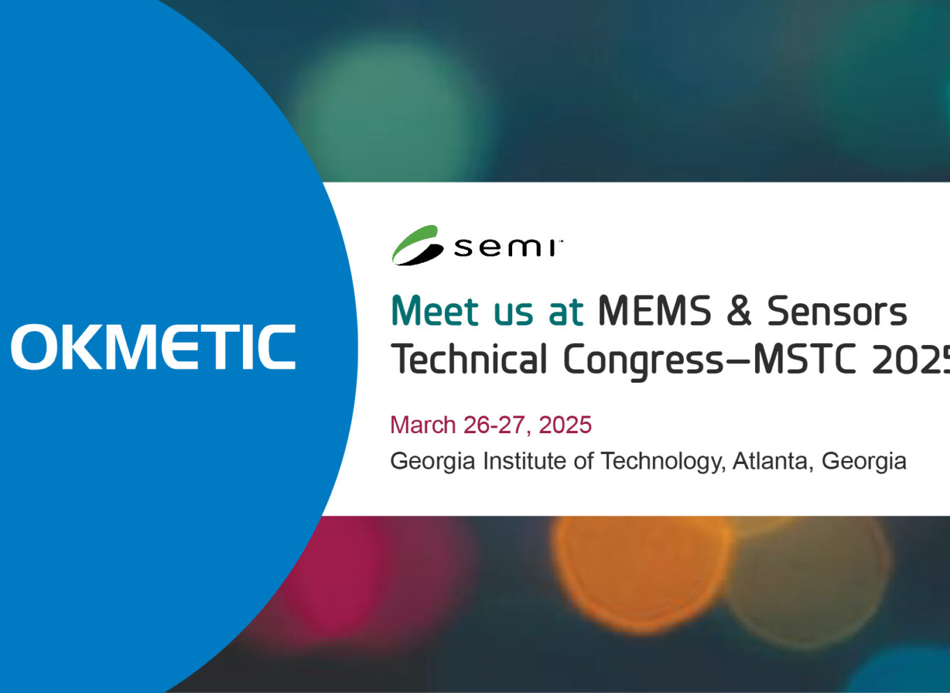
  • Display all
  • Career stories
  • Insights
  • News
  • Product news

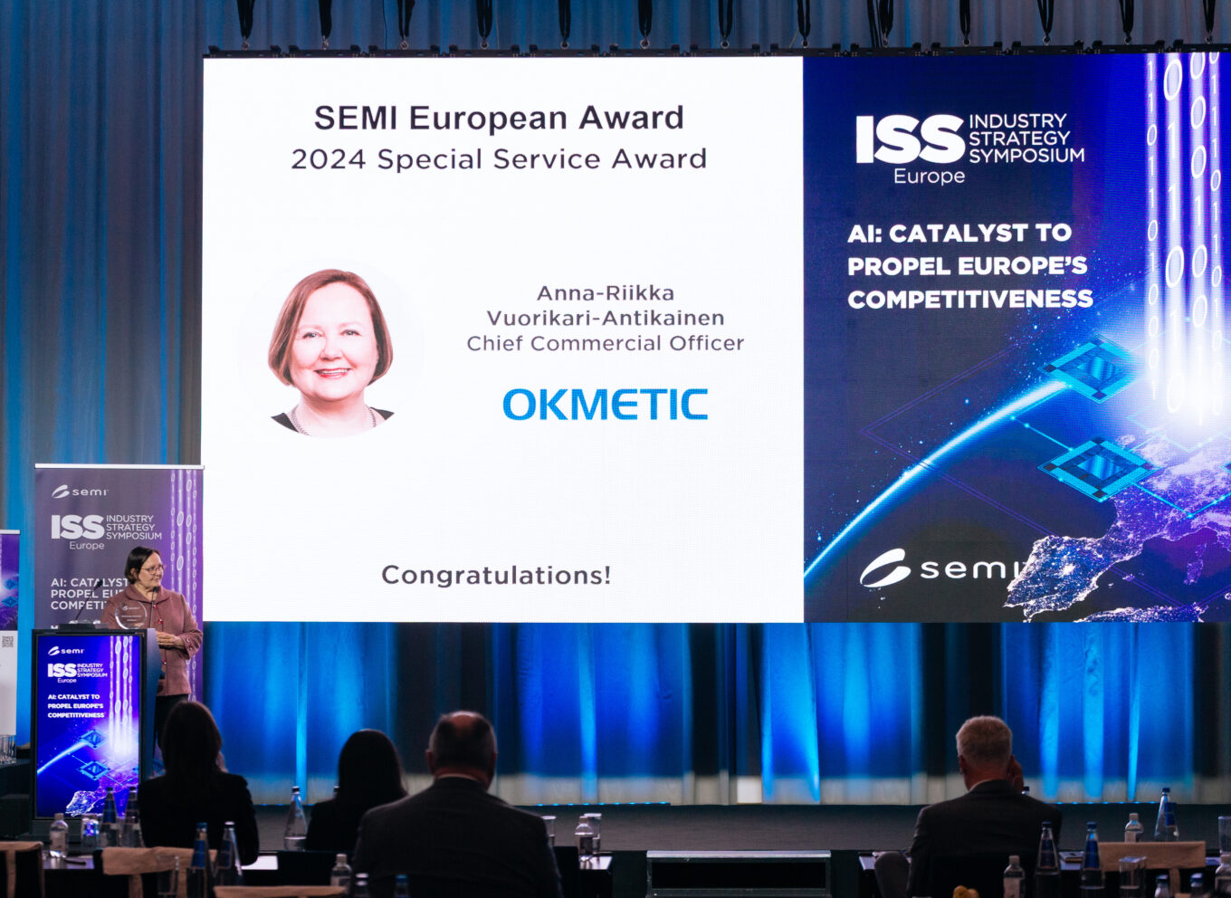
Okmetic CCO receives SEMI Europe Special Service Award

Okmetic participating in Semicon Korea

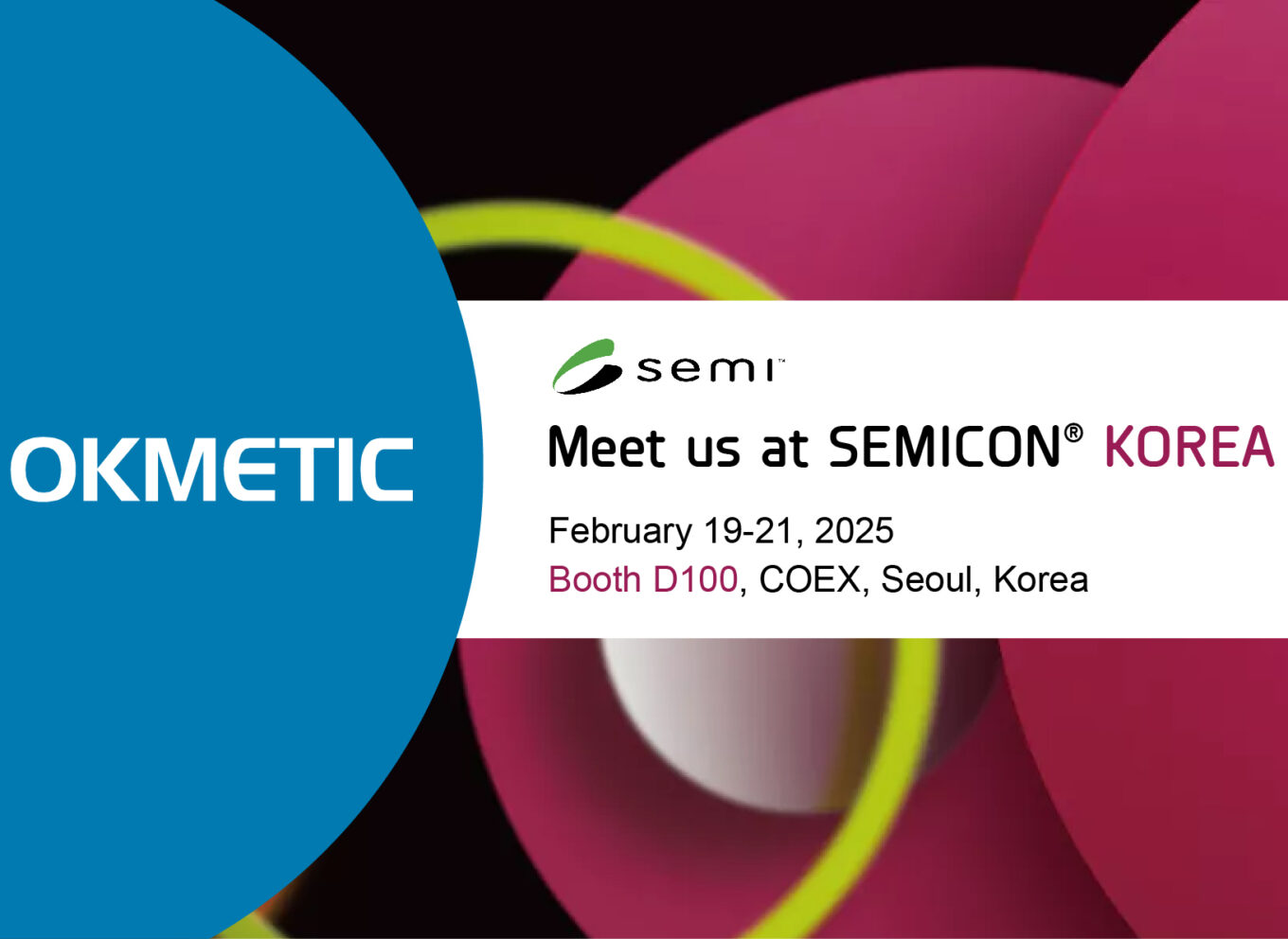
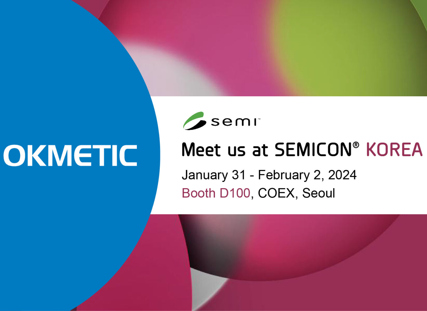
Okmetic is participating in SEMICON® Korea!  

Okmetic participating SPIE Photonics West

Okmetic participating in CMC Seminar 23 October

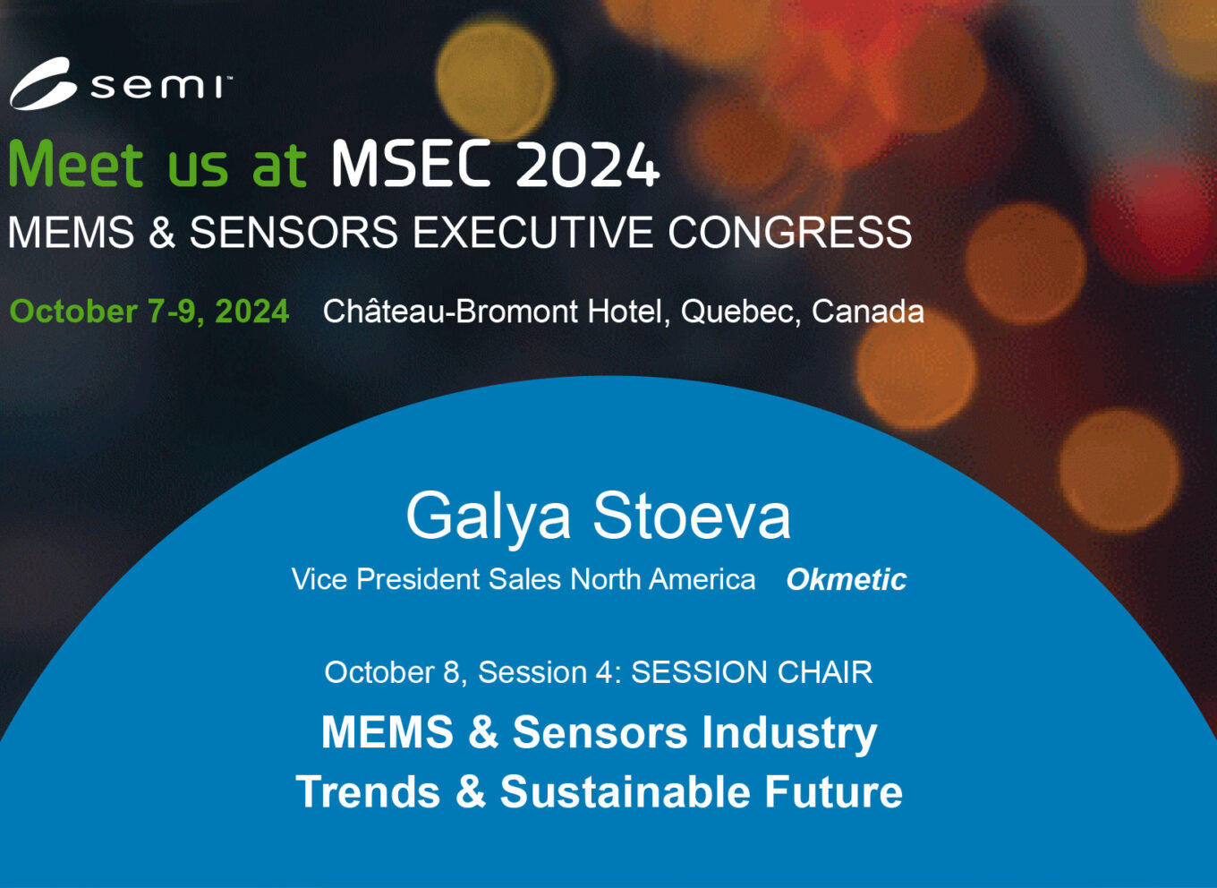
Okmetic is participating in MSEC

Okmetic will be participating in ISES US Power

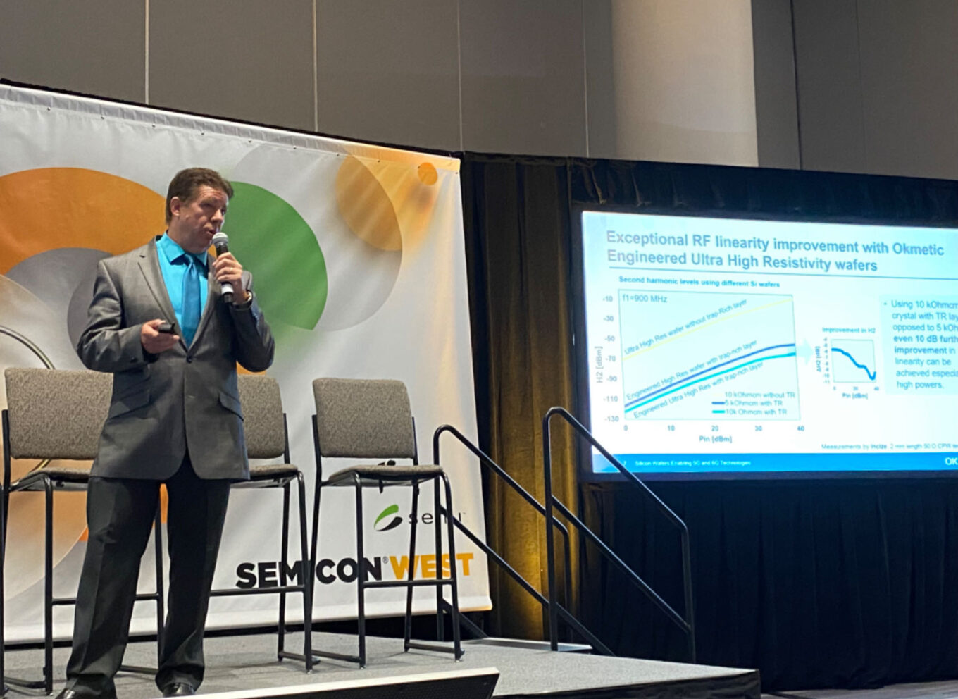
Jim Reed held a speech at Semicon West 2024

Join Okmetic at IMS2024 on 16-21 June 2024, in Washington, DC

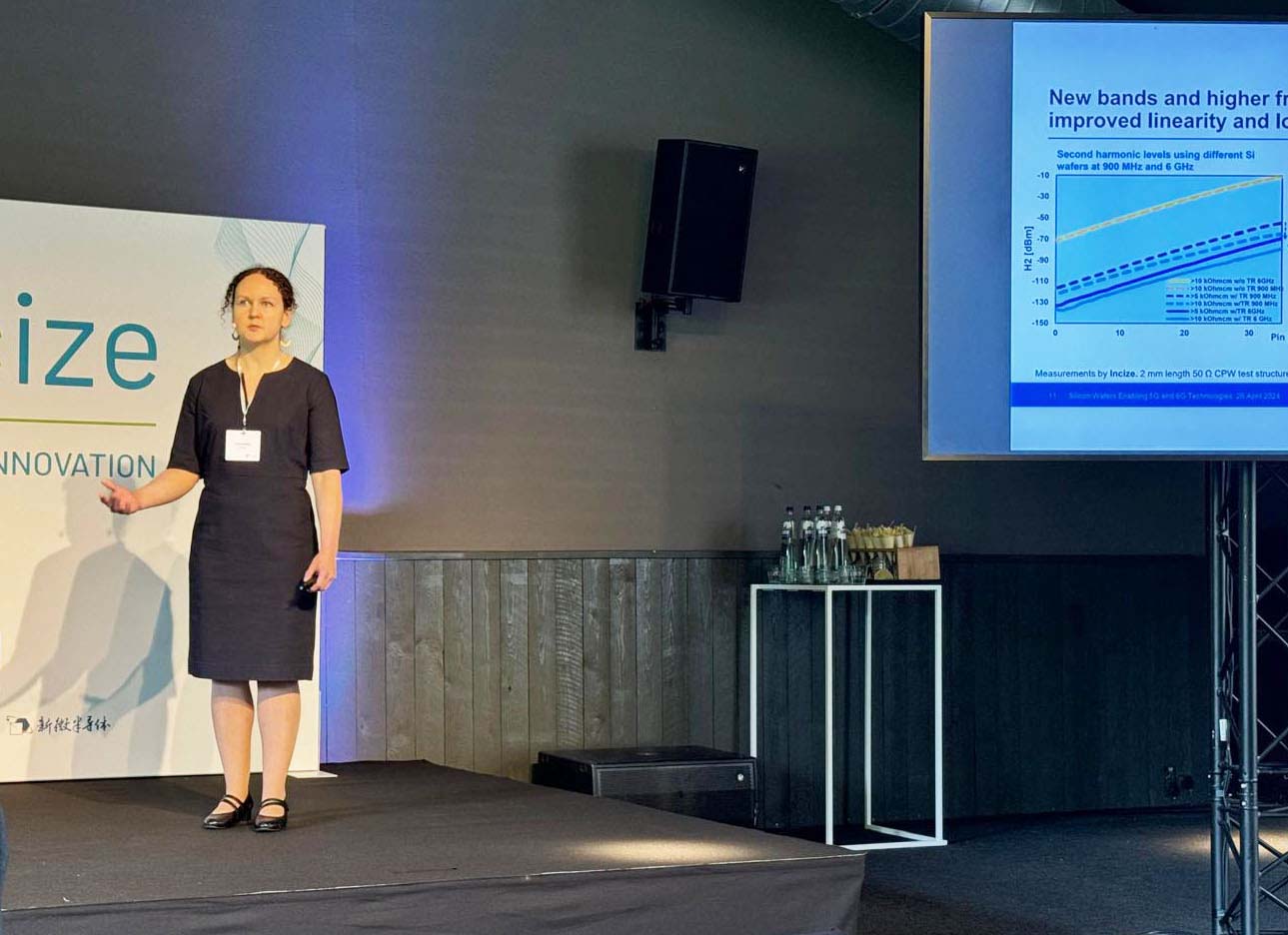
Katja Parkkinen held a speech at Incize RF Workshop

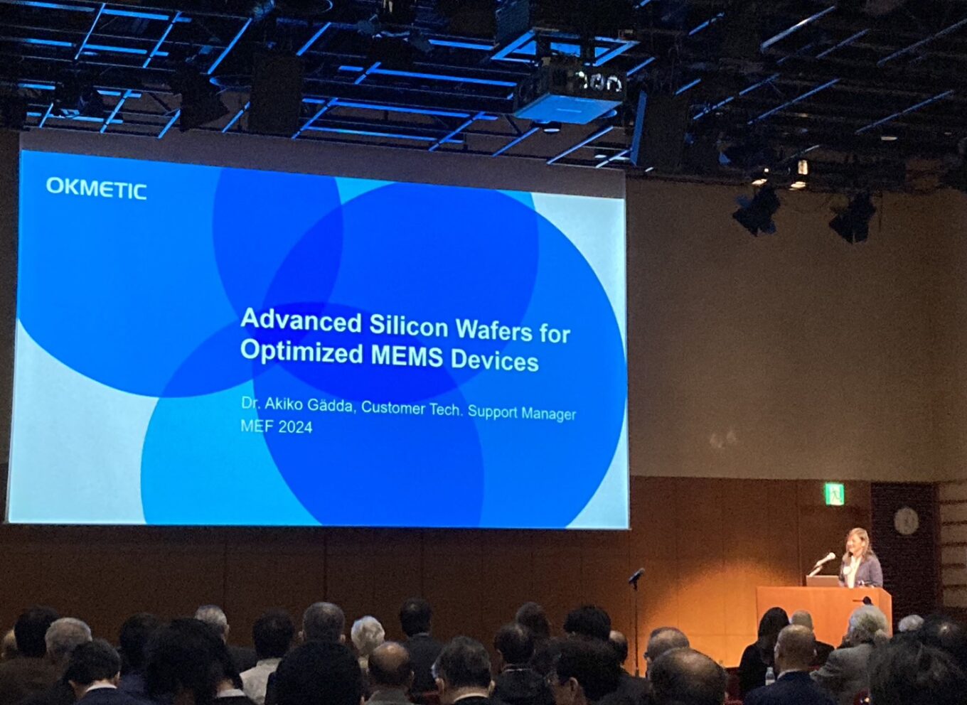
Dr. Akiko Gädda gave a speech at the MEF

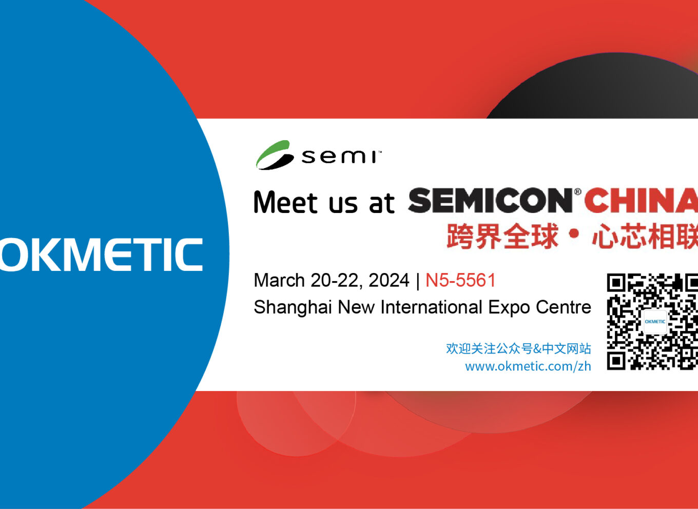
Okmetic is participating in the SEMICON China 2024 during March 20-22 in Shanghai

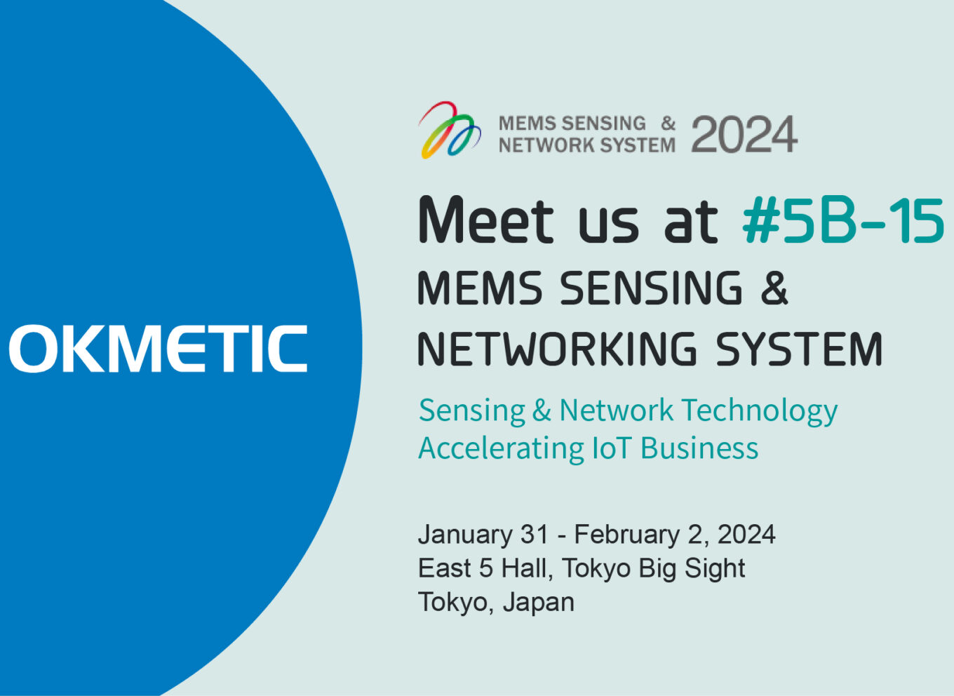
Okmetic is participating in the MEMS Sensing and Network System in Tokyo

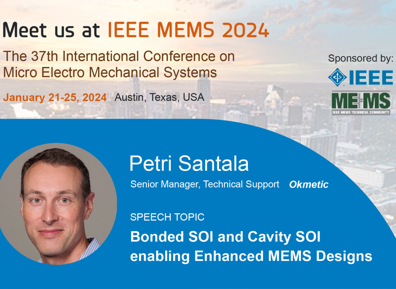
Okmetic is participating in the IEEE MEMS Conference 2024, to be held in Austin, Texas

Okmetic is participating SEMICON® KOREA from January 31-February 2

Okmetic participating in Semicon Europa

  • Previous
  • 1
  • 2
  • 3
  • 4
  • 5
  • Next
  • Column
    • Silicon Wafers 150-200 mm
    • Silicon Wafers 300 mm
    • Applications
To front page
  • About Okmetic
  • Contact Us
  • Quality
  • Sustainability
  • Work with Us
  • Privacy Policy and Terms of Use
  • Safety Data Sheet
LinkedIn YouTube WeChat Facebook