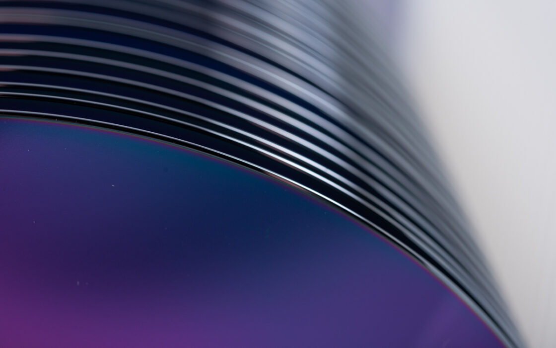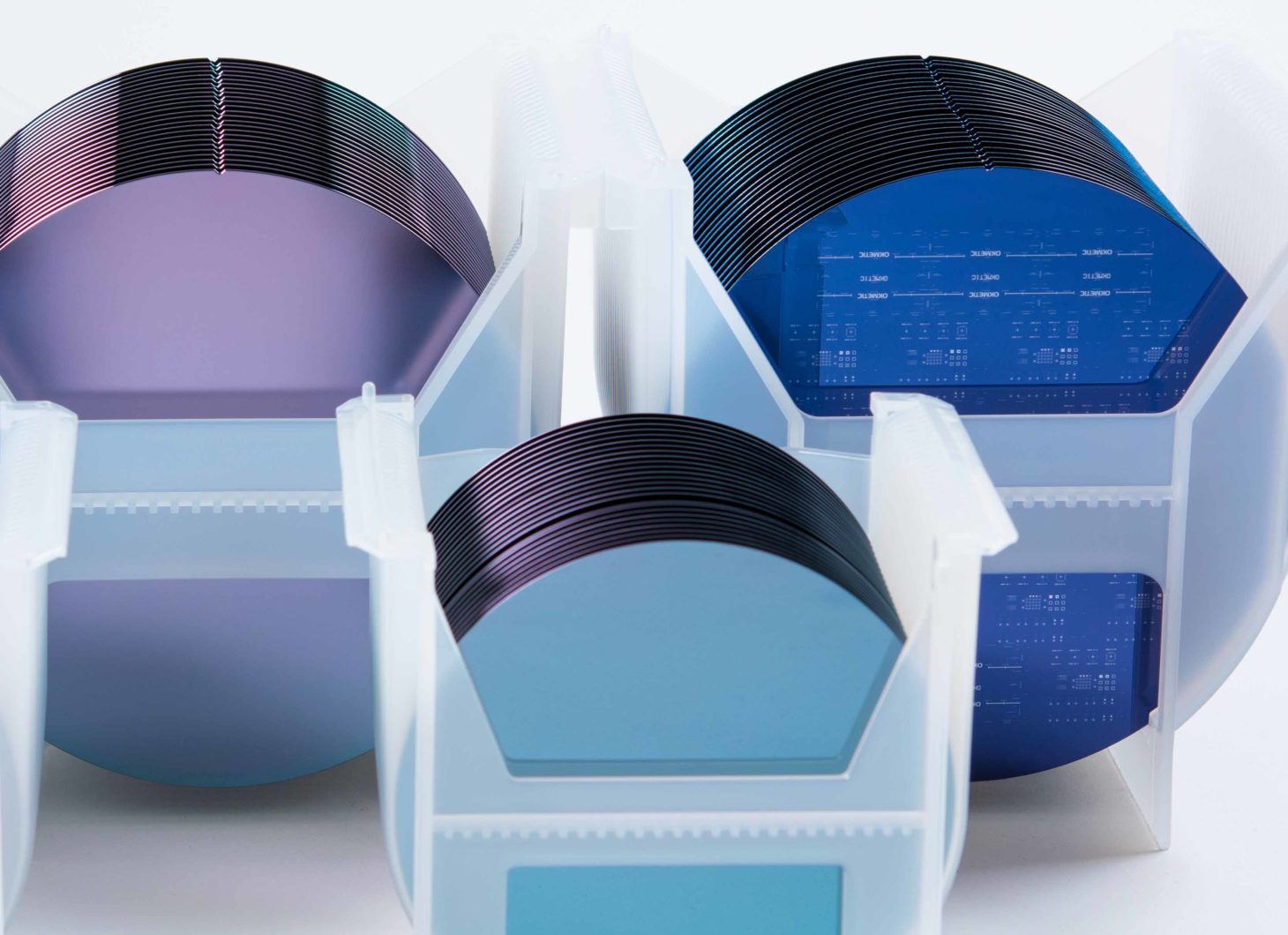
SOI wafers – Silicon-On-Insulator line
Produced with over 20 years’ of expertise Okmetic’s comprehensive line of bonded Silicon On Insulator (SOI) wafers provides an optimal platform for the manufacture of demanding MEMS, sensor, power and RF devices. Okmetic SOI wafers enable additional design freedom, maximum device performance, cost-effectiveness and ease of manufacturing.
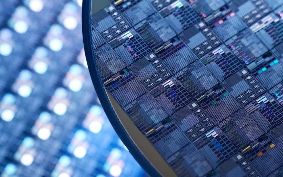
Okmetic was among the first silicon wafer suppliers to introduce Silicon On Insulator technology and SOI wafers to MEMS industry, and now the company has been volume producing SOI wafers for over 20 years already. SOI wafers are silicon wafers with a thin silicon film on insulating oxide, and their production requires a very high level of technical expertise. SOI wafers enable the manufacture of the most advanced MEMS, sensor, power and RF devices used in automotive and healthcare applications, smart wristbands, smartphones and tablets as well as applications related to Internet of Things (IoT) utilizing sensor-provided data in device-to-device communication.
SOI wafers provide an optimal platform for the manufacture of MEMS, sensor, power and RF devices
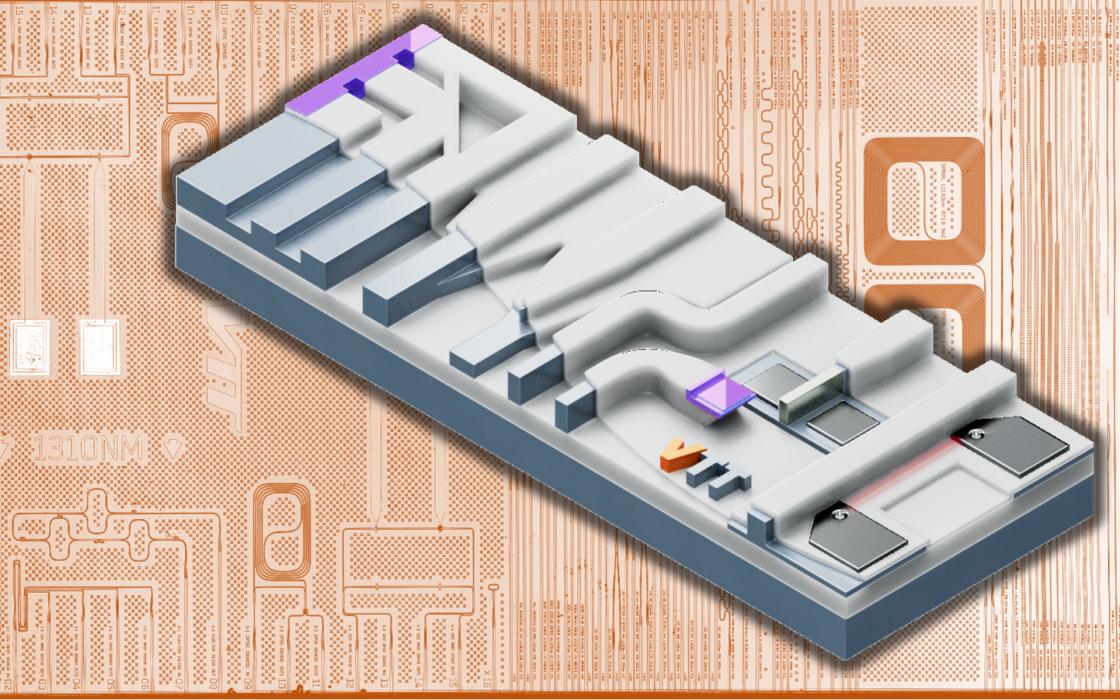
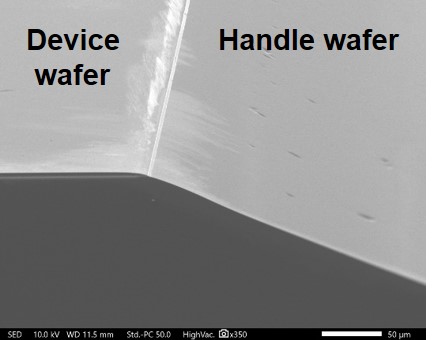
Okmetic’s Silicon On Insulator (SOI) wafers are manufactured by bonding technology. Two silicon wafers are bonded together leaving an insulating oxide layer between them. Typically, sensing elements and IC devices are built on the top device layer. The buried oxide layer is an excellent electric insulating layer and an effective etch-stop, but can be used as a sacrificial layer as well. The bottom handle wafer is supporting the structure, but can also be utilized in sealing the structure or as part of the sensing element or the device.
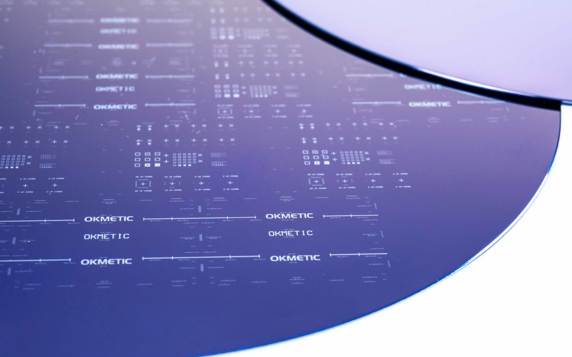
Comprehensive line of Silicon On Insulator (SOI) wafers
Okmetic’s SOI wafers are manufactured entirely in-house which allows us to monitor critical crystal and wafer parameters to ensure the highest quality of SOI wafers. The widest wafer portfolio on the market enables the selection of e.g. optimal electrical conductivity and different crystallographic orientations to ensure better utilization of the anisotropic properties of silicon. Our sales and technical support are happy to help you find an optimal solution, customized for your needs.
Okmetic’s SOI wafer line comprise the following products:
- BSOI wafers – Bonded SOI (including BSOI variations 0.3 SOI, DSOI, LSOI and Thick SOI)
- C-SOI® wafers – Cavity SOI (including C-SOI® variations EC-SOI, Double C-SOI®, C-SOI® with patterned device layer, C-SOI® with poly via)
- E-SOI® wafers – Enhanced SOI with tight thickness uniformity
- Terrace Free SOI capability for BSOI, E-SOI® and Power Management SOI wafers
- High Resistivity BSOI wafers are part of our RFSi® wafer line
- Power Management SOI wafers are part of our Power wafer line
Typical SOI specifications
| Growth method | Cz, MCz, A-MCz® |
| Diameter | 200 mm, 150 mm |
| Crystal orientation | <100>, <110>,<111> |
| N type dopants | Antimony, Phosphorus |
| P type dopants | Boron |
| Resistivity1 | From <0.001 to >7,000 Ohm-cm* *Resistivity range varies by dopant and orientation |
| Device layer thickness2* | From 1 μm to >200 μm Tolerance ±0.5 μm (standard BSOI), ±0.3 μm (0.3 SOI), ±0.1 μm (E-SOI®, Power Management SOI), ±0.5 μm or lower (C-SOI®) |
| Buried oxide layer thickness3 | From 0.3 μm to >5 μm |
| Handle wafer thickness4 | 200 mm: 300 μm to 950 μm 150 mm: 300 μm to 950 μm |
| Back surface | Polished or etched |
| Terrace area | Standard or Terrace Free (Available for 200 mm BSOI, E-SOI® and Power Management SOI) |
2Other thicknesses possible with certain limitations. 150 mm E-SOI® tolerance ±0.2 µm
3Type: thermal oxide. Typically 0.5 μm to 2 μm. >5 μm BOX possible with certain limitations.
4200 mm: typically 500-725 μm, 150 mm: typically 380-675 μm. ±3 µm tolerance for demanding devices
*Possibility also for two device and buried oxide layers with different thicknesses.
Fully CMOS compatible wafer surface quality and cleanliness requirements
Okmetic – Technology leader in Silicon On Insulator wafers
Okmetic is a true pioneer in the field of Silicon On Insulator (SOI) wafers as the company started to develop SOI technology for the MEMS industry already in the 1990’s and has been volume producing SOI wafers ever since 2001. The MEMS industry was the first to adopt the new Silicon On Insulator wafer technology and it continues to be the main growth driver for SOI wafer demand. Over the years, SOI wafers have also expanded to power management solutions utilizing trench isolation technologies such as high voltage BCD and lateral HV devices. SOI wafers are also used in the RF field for the needs of which Okmetic has designed High Resistivity BSOI wafers.
2023 Launch of Terrace Free SOI capability
2021 Okmetic SOI 20th anniversary
2020 EC-SOI wafer combining E-SOI® and C-SOI® benefits
2019 New C-SOI® wafer production line
2016 Launch of E-SOI® wafer
2015 SOI wafers for power management
2010 SOI-based extremely small pressure sensors and wearable electronics
2009 C-SOI® wafers in volume production
2008 SOI-based silicon microphones
2006 C-SOI® -based inertial sensors for automotive industry
2005 First C-SOI® wafer deliveries
2001 SOI wafer production line started
1998 Okmetic SOI technology established