Engineered High Resistivity wafers with trap-rich layer
Okmetic Engineered High Resistivity SSP and DSP wafers combine low Oi and up to >7,000 Ohm-cm resistivities with trap-rich layer. Thanks to this combination, the Engineered High Resistivity silicon wafers enable superior RF device performance and very low insertion losses.
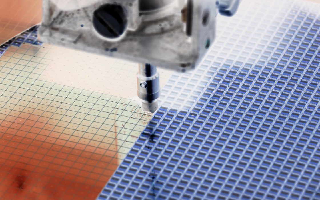
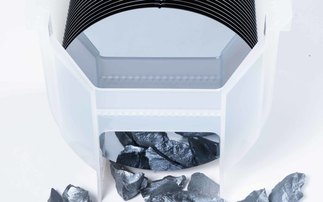
Okmetic Engineered High Resistivity silicon wafers are manufactured with Advanced Magnetic Czochralski (A-MCz®) crystal growth method and they combine low Oi and up to >7,000 Ohm-cm resistivity with engineered trap-rich layer. Tailored for the needs of RF filters and devices, this cutting-edge wafer technology reduces RF losses and provides stable “effective resistivity” over frequency range, resulting in higher Q values. The Engineered High Resistivity wafers also help improve linearity over temperature, minimize intermodular and second harmonics distortion, and reduce characteristic stress and bow. In case you are looking for close to zero substrate-induced losses for your RF device using Engineered Ultra High Resistivity wafers as platform is highly recommended. Find out more about our Engineered high resistivity wafer benefits in our White paper “Advancing from 4G LTE to 5G and 6G: Engineered RFSi® silicon wafers for high-performance RF devices.
Engineered High Resistivity wafers provide superior performance in terms of 2nd harmonics and intermodular distortion, Insertion losses and Q-values
Filters and IPD devices among main usage areas
Engineered High Resistivity wafers are widely used in membrane type Bulk Acoustic Wave (BAW) filters such as FBAR, XBAR and BAW FMR, and high-performance Surface Acoustic Wave (SAW) filters such as TF-SAW, TC-SAW, POI-SAW, ML-SAW and Integrated Passive Device (IPD) applications as the proprietary trap-rich layer enables high effective resistivity, very low insertion losses, superior 2nd harmonic values as well as excellent linearity. In addition, Engineered High Resistivity wafers can also be used as capping wafers for acoustic filters. Other usage areas include integrated RFIC applications and silicon interposers, the both of which benefit from the very high and stable resistivity and superior electrical performance provided by customized High Resistivity wafers.
Engineered High Resistivity wafers with 5 kOhm-cm resistivity reach very low H2 levels of even <-85 dBm
Optimized, superior performance and lower Total Cost of Ownership:
- Excellent results observed in both IPD, BAW and TF-SAW filter manufacturing.
- Engineered High Resistivity wafers with 5 kOhm-cm resistivity and trap-rich layer reach very low H2 levels of even <-85 dBm.
- Engineered High Resistivity wafers provide excellent IMD3 (third order intermodulation distortion) suppression.
- The engineered trap-rich layer can be tailored to match the specific customer process to maximize the gains in harmonic behavior and overall losses.
- No need for complex implants and their effects on supply chain. The engineered trap-rich layer is purely silicon-based providing a good match for the customers’ production lines as no foreign materials are involved.
Customized, Engineered High Resistivity solutions
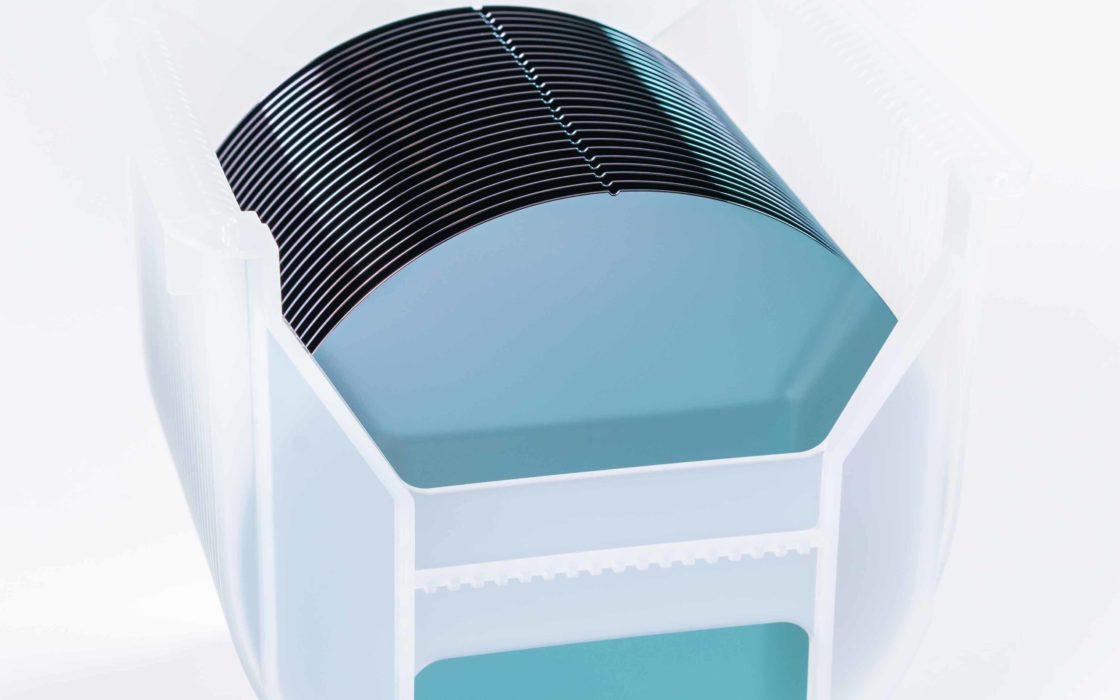
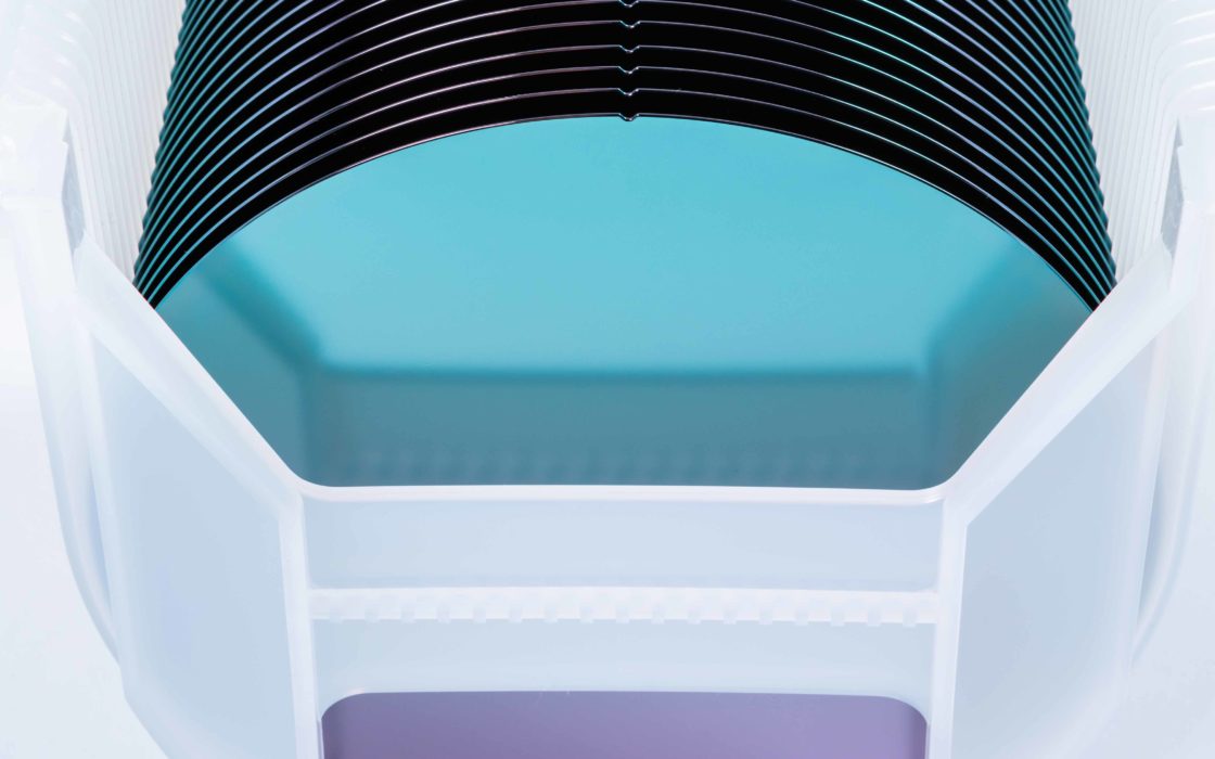
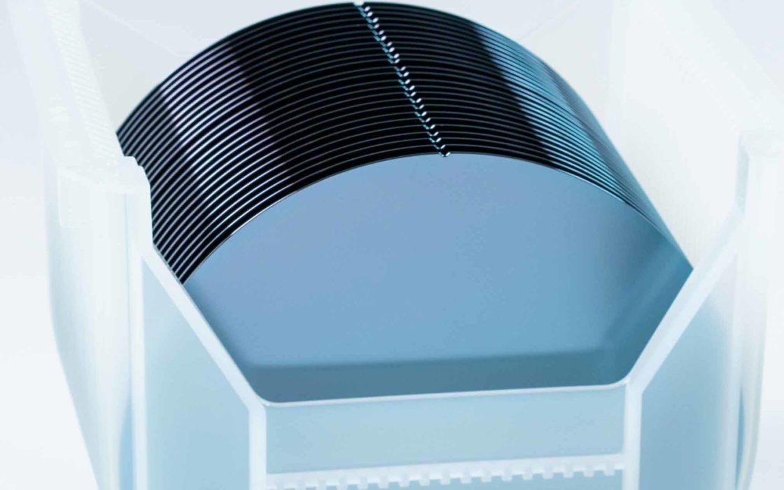
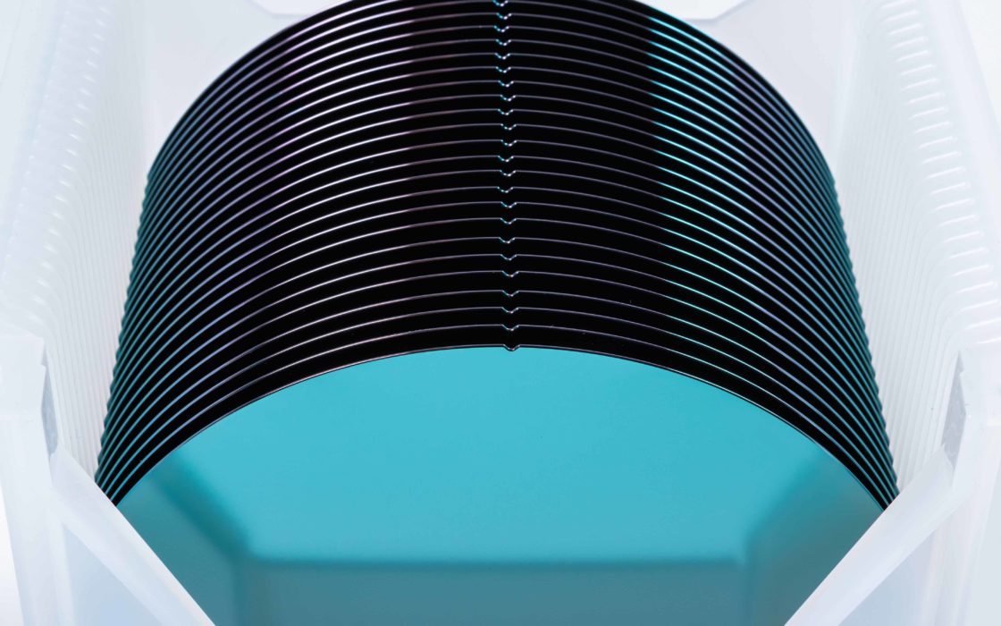
Okmetic Engineered High Resistivity wafers are optimized, A-MCz® silicon wafers with low Oi, up to >7,000 Ohm-cm resistivity and engineered trap-rich layer to further minimize RF losses. These extremely high resistivities are enabled by Okmetic’s trademark Advanced Magnetic Czochralski (A-MCz®) crystal growth method. In addition to resistivities also other wafer parameters can be adjusted. The Engineered High Resistivity wafer selection includes 150 to 200 mm SSP and DSP silicon wafers doped with either Boron or Phosphorus. Crystal orientations include <100> and <111> and thicknesses range from 380 to >1,150 µm.
Engineered High Resistivity wafer specifications
| Growth method | MCz, A-MCz® |
| Diameter | 150 mm, 200 mm |
| Crystal orientation | <100>, <111> |
| N type dopants | Phosphorus |
| P type dopants | Boron |
| Resistivity | Up to >7,000 Ohm-cm*, Engineered Ultra High Resistivity wafers for over 10 kOhm-cm resistivity *Resistivity range varies by dopant and orientation |
| Oxygen | Typically ≤5 ppma or ≤10 ppma (ASTM F121-83). Can be optimized to Customer process. |
| SSP (etched backside) wafer thickness | 200 mm: 550 to 1,150 µm* 150 mm: 400 to 1,150 µm *Other thicknesses possible with certain limitations |
| DSP (polished backside) wafer thickness | 200 mm: 380 to >1,150 µm* 150 mm: 380 to >1,150 µm *Other thicknesses possible with certain limitations |
| Trap-rich layer | Purely silicon-based, no foreign materials |
See all 150-200 mm silicon wafers