Skip to content
To front page
  • Silicon Wafers
    • MEMS Wafer Line
      • MEMS SSP and DSP Wafers
      • Selecting the ideal wafer for MEMS devices: Balancing cost, performance, and manufacturing efficiency
    • RFSi® Wafer Line – High Resistivity for RF
      • High Resistivity Wafers
      • Engineered High Resistivity Wafers with Trap-Rich Layer
      • Engineered Ultra High Resistivity wafers
      • UF-RFSi® – Ultra Flat High Resistivity Wafers
      • High Resistivity BSOI Wafers
      • RF GaN Substrate wafers
    • Power Wafer Line
      • Power Management SOI wafers
      • Power GaN Substrate wafers (Si and SOI) 
      • Discrete Power Device wafers 
    • SOI Wafers – Silicon-On-Insulator Line
      • BSOI Wafers – Bonded SOI
      • C-SOI® Wafers – Cavity SOI
      • E-SOI® Wafers – Enhanced SOI
      • Terrace Free SOI wafers
    • Patterned Wafers – DRIE and Lithography
    • TSV Wafers – Through Silicon Via
    • DSP Wafers – Double Side Polished
    • SSP Wafers – Single Side Polished
    • Customized Wafers and Prototyping
    • Production and Capacity Expansion 
    • Supplier Awards and Collaboration Projects
  • Applications
    • MEMS and Sensors
    • RF Filters and Devices
    • Power Devices
  • Quality and Responsibility
    • Quality
      • Quality Policy
      • Quality Tools
        • Artificial Intelligence at Okmetic
        • 5S at Okmetic
    • Sustainability
      • Responsibility for Personnel
      • Responsibility for Safety and Health
      • Responsibility for Environment
      • Business Ethics
      • Managing Responsibility
      • Reports on Responsibility
    • Certificates
  • Work with Us
    • Production Experts
    • Semiconductor Professionals
    • Students
    • Maintenance professional
    • Technical professionals
    • Sales and technical support
    • Open Positions
  • About Okmetic
    • Company
    • Strategy and Values
    • Executive Management Group
    • Investments
    • Research and Development Work
    • Tale of a Silicon Wafer
    • The History of Okmetic
    • News & Insights
    • Contact Us
  • English
    • Suomi
    • 日本語
    • 中文 (中国)

Events

Okmetic+About Okmetic+News & insights+Events

Select content category

  • Display all
  • Career stories
  • Insights
  • News
  • Product news

Okmetic is sponsoring and attending MEF 2023 to be held on April 20-21 in Tokyo

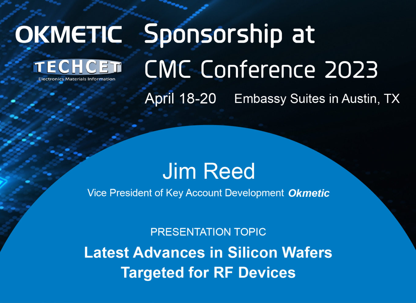
Okmetic’s Vice President of Key Account Development Jim Reed will be giving a speech at CMC Conference 2023

Okmetic is attending APEC 2023 held in Orlando during March 19-23, 2023

Okmetic CTO Atte Haapalinna to give a presentation at ISES USA 2023

Okmetic is participating SEMICON® KOREA during February 1-3, 2023

Okmetic is participating Medical Wearables 2022 during December 6-8

Okmetic is participating SEMICON Europa 2022 on 15-18 November

Okmetic is sponsoring the CMC F2F event on 14-16 November

Okmetic is sponsoring the WaferBond’22 conference on 5-6 October

Customer Support Manager Akiko Gädda is giving a speech at the MEMS & Imaging Sensors Summit on 6-7 September

Okmetic is sponsoring MEMS World Summit held in Lake Maggiore on 23-24 June

Okmetic sponsoring and speaking at the CMC Conference on 27-29 April

Okmetic is the silver sponsor of MSTC held on 26-27 April

Okmetic sponsoring MEF Japan on 20-21 April

CTO Atte Haapalinna giving a speech at European Microwave Week on 4 April 2022

  • Previous
  • 1
  • 2
  • 3
  • 4
  • 5
  • Next
  • Silicon Wafers
    • Column
      • SOI Wafers – Silicon-On-Insulator Line
      • Patterned Wafers – DRIE and Lithography
      • TSV Wafers – Through Silicon Via
    • Column
      • RFSi® Wafers – High Resistivity Line for RF
      • SSP Wafers – Single Side Polished
      • DSP Wafers – Double Side Polished
    • Column
      • Power wafer line
      • Customized Wafers and Prototyping
      • Production and Subcontracting
To front page
  • About Okmetic
  • Contact Us
  • Applications
  • Quality and Responsibility
  • Work with Us
  • Privacy Policy and Terms of Use
  • Safety Data Sheet
LinkedIn YouTube WeChat Facebook