Skip to content
To front page
  • Silicon Wafers
    • MEMS Wafer Line
      • MEMS SSP and DSP Wafers
      • Selecting the ideal wafer for MEMS devices: Balancing cost, performance, and manufacturing efficiency
    • RFSi® Wafer Line – High Resistivity for RF
      • High Resistivity Wafers
      • Engineered High Resistivity Wafers with Trap-Rich Layer
      • Engineered Ultra High Resistivity wafers
      • UF-RFSi® – Ultra Flat High Resistivity Wafers
      • High Resistivity BSOI Wafers
      • RF GaN Substrate wafers
    • Power Wafer Line
      • Power Management SOI wafers
      • Power GaN Substrate wafers (Si and SOI) 
      • Discrete Power Device wafers 
    • SOI Wafers – Silicon-On-Insulator Line
      • BSOI Wafers – Bonded SOI
      • C-SOI® Wafers – Cavity SOI
      • E-SOI® Wafers – Enhanced SOI
      • Terrace Free SOI wafers
    • Patterned Wafers – DRIE and Lithography
    • TSV Wafers – Through Silicon Via
    • DSP Wafers – Double Side Polished
    • SSP Wafers – Single Side Polished
    • Customized Wafers and Prototyping
    • Production and Capacity Expansion 
    • Supplier Awards and Collaboration Projects
  • Applications
    • MEMS and Sensors
    • RF Filters and Devices
    • Power Devices
  • Quality and Responsibility
    • Quality
      • Quality Policy
      • Quality Tools
        • Artificial Intelligence at Okmetic
        • 5S at Okmetic
    • Sustainability
      • Responsibility for Personnel
      • Responsibility for Safety and Health
      • Responsibility for Environment
      • Business Ethics
      • Managing Responsibility
      • Reports on Responsibility
    • Certificates
  • Work with Us
    • Production Experts
    • Semiconductor Professionals
    • Students
    • Maintenance professional
    • Technical professionals
    • Sales and technical support
    • Open Positions
  • About Okmetic
    • Company
    • Strategy and Values
    • Executive Management Group
    • Investments
    • Research and Development Work
    • Tale of a Silicon Wafer
    • The History of Okmetic
    • News & Insights
    • Contact Us
  • English
    • Suomi
    • 日本語
    • 中文 (中国)

News

Okmetic+About Okmetic+News & insights+News

Select content category

  • Display all
  • Career stories
  • Events
  • Insights
  • Product news

Thank you for 2022

Okmetic renewed its values

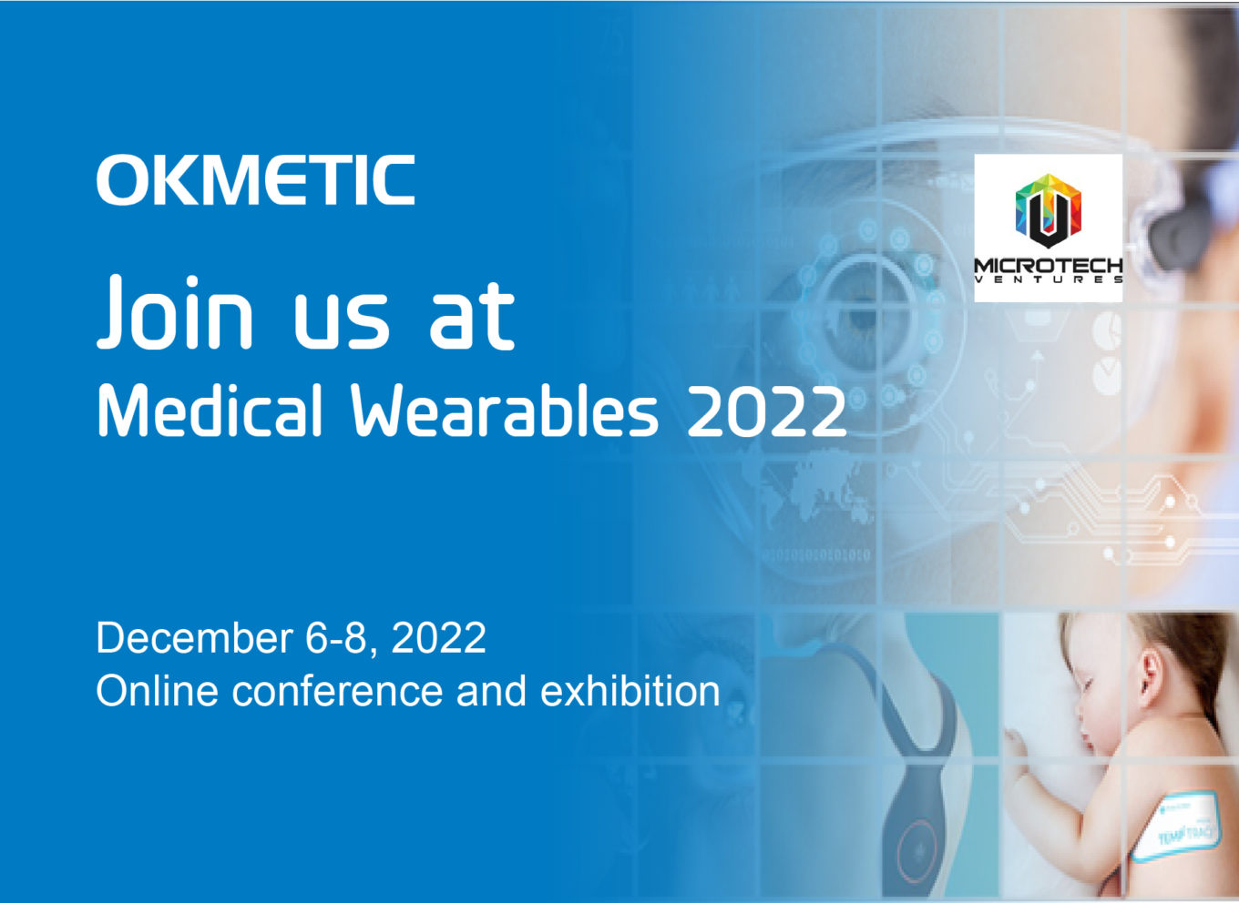
Okmetic is participating Medical Wearables 2022 during December 6-8

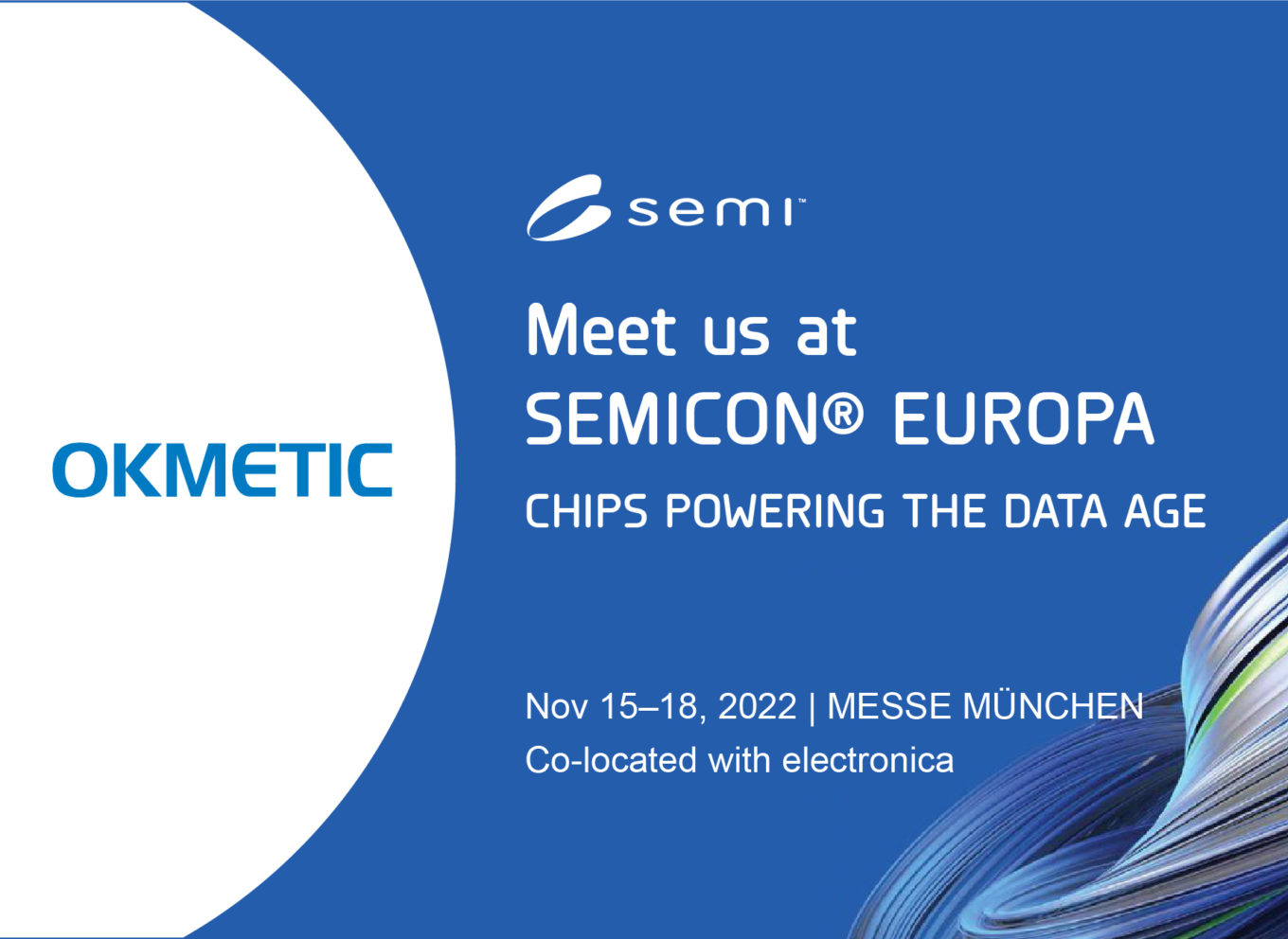
Okmetic is participating SEMICON Europa 2022 on 15-18 November

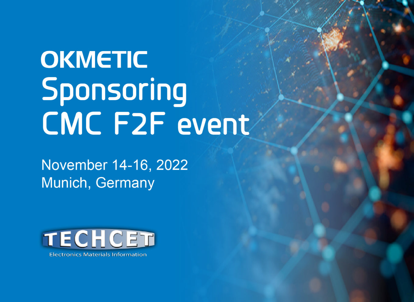
Okmetic is sponsoring the CMC F2F event on 14-16 November

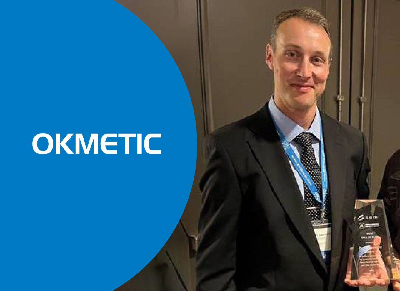
Okmetic Customer Support Manager Petri Santala inducted in the SEMI-MEMS & Sensors Industry Group Hall of Fame

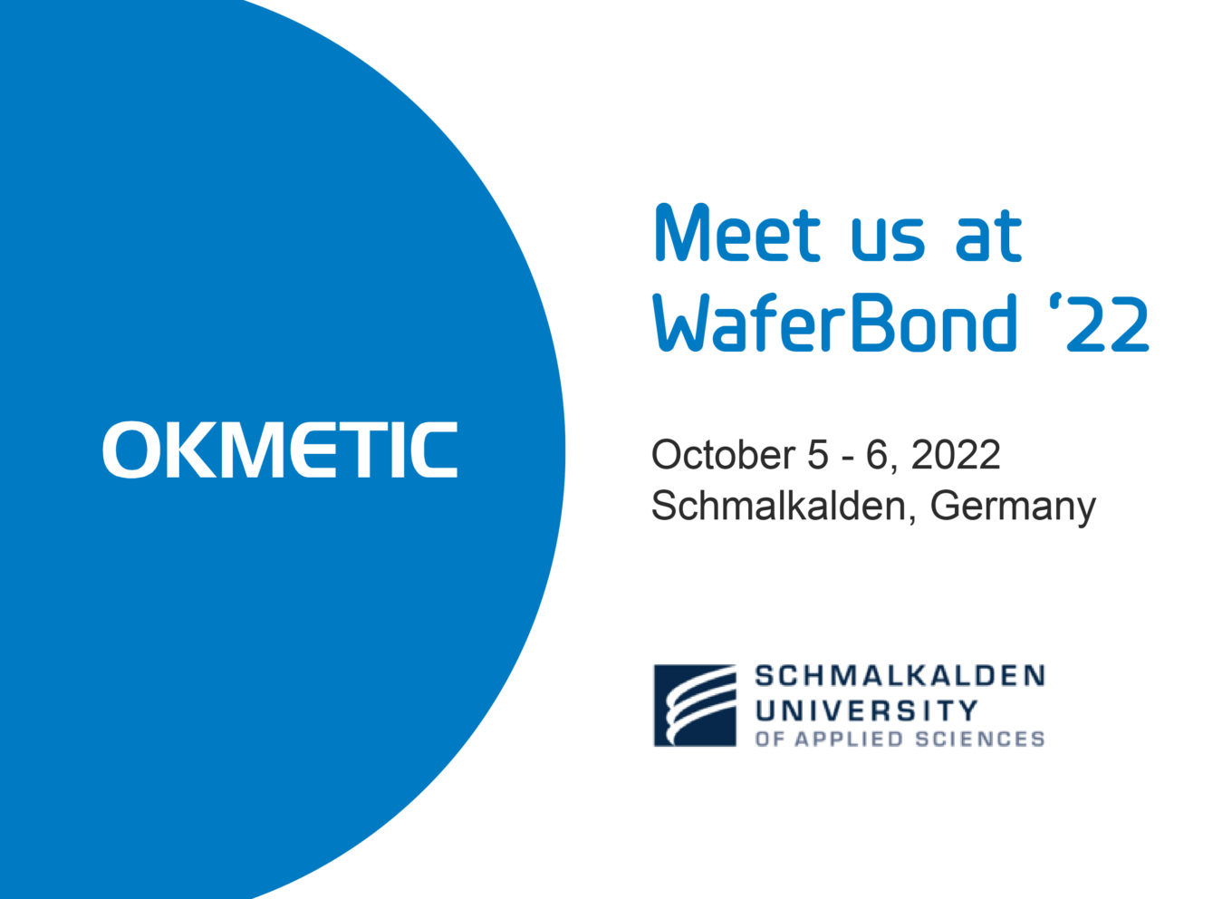
Okmetic is sponsoring the WaferBond’22 conference on 5-6 October

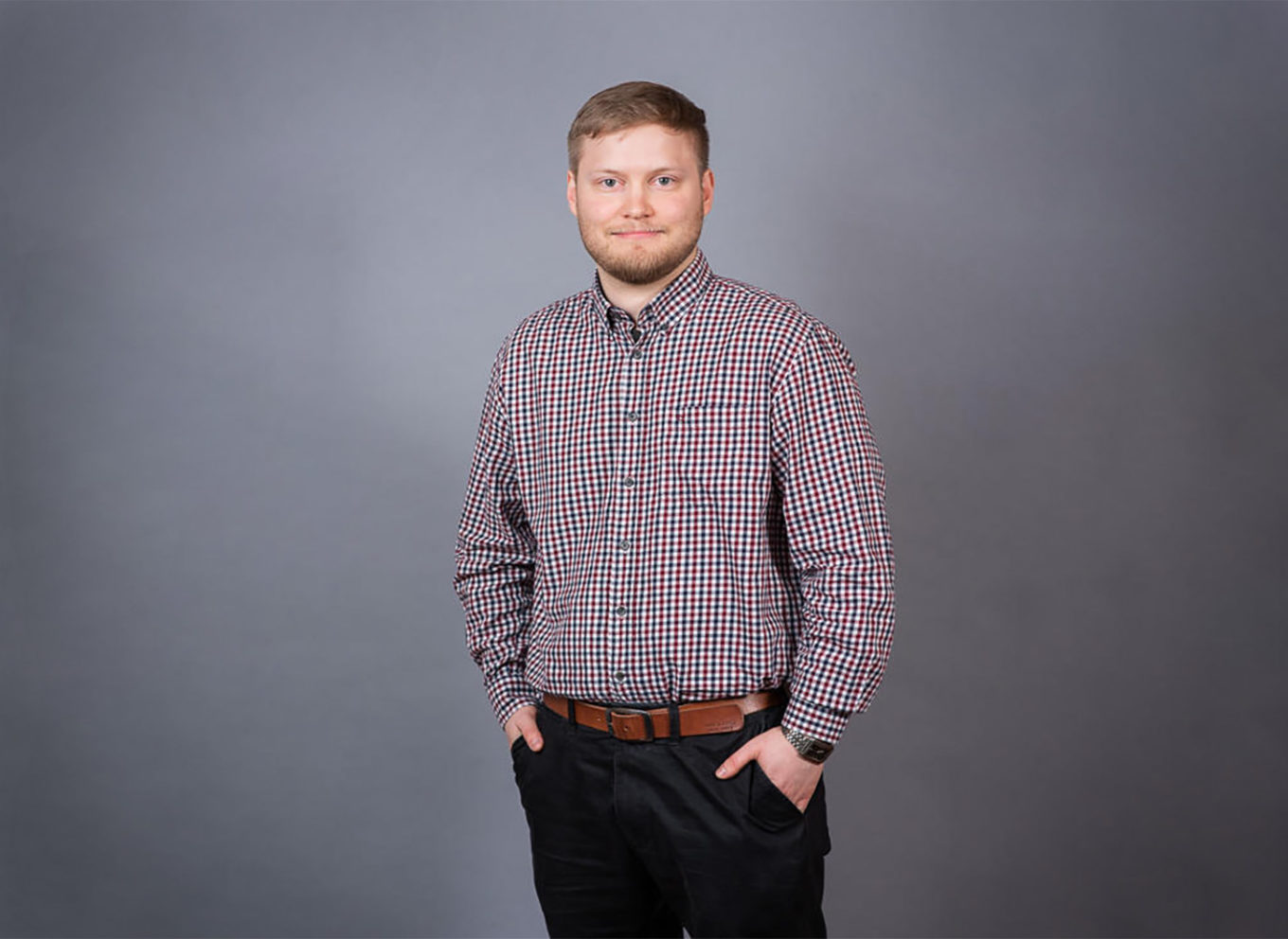
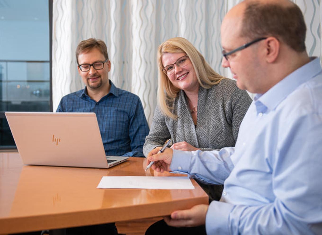
Jonne Vähänissi: “Okmetic is the best place for a process development engineer to work in Finland.”

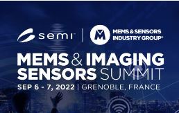
Customer Support Manager Akiko Gädda is giving a speech at the MEMS & Imaging Sensors Summit on 6-7 September

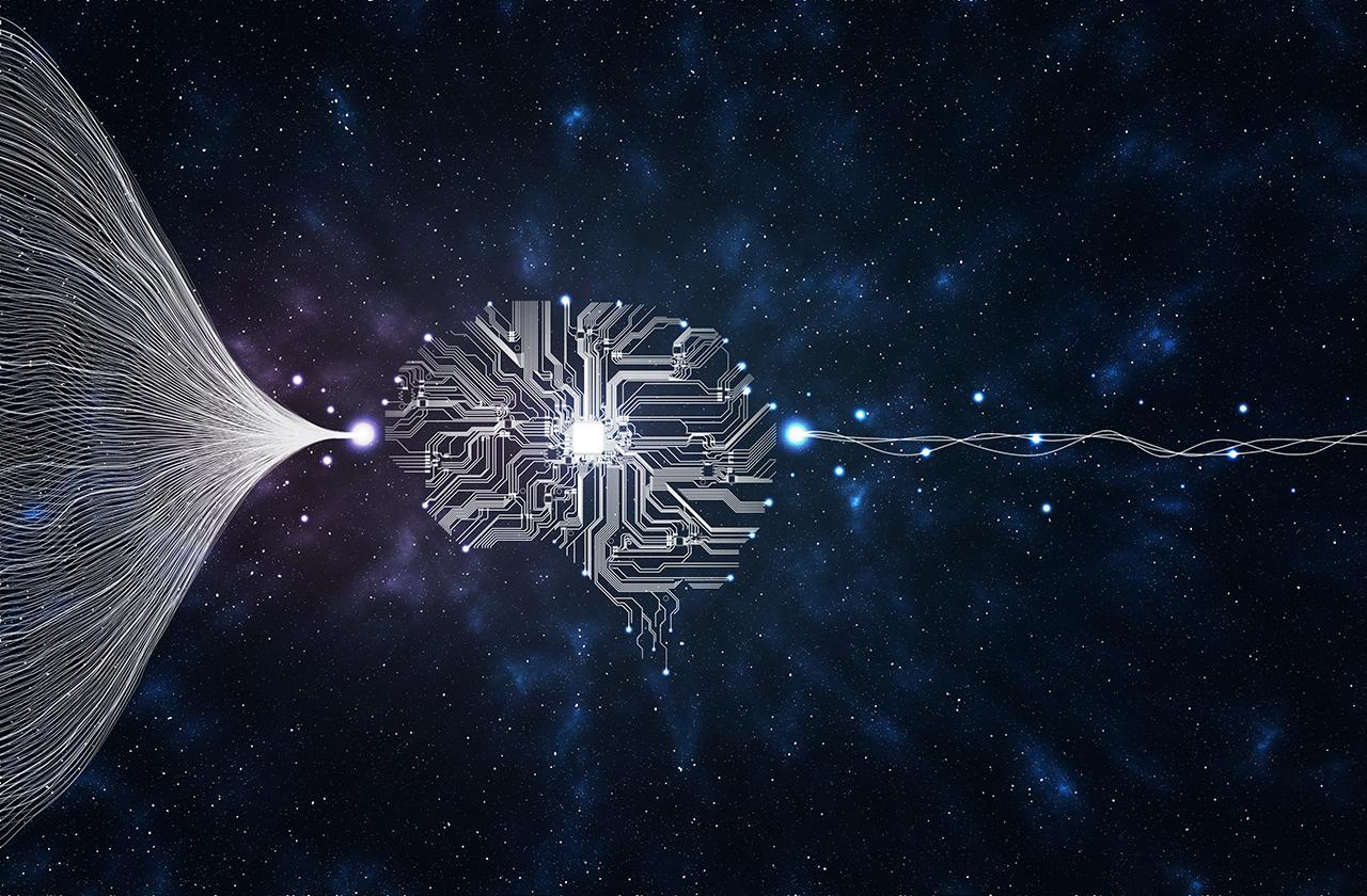
Okmetic On-Demand Webinar: Improving the quality of electronics components and systems with AI

Okmetic participated in Position II project developing next generation smart catheters and implants 

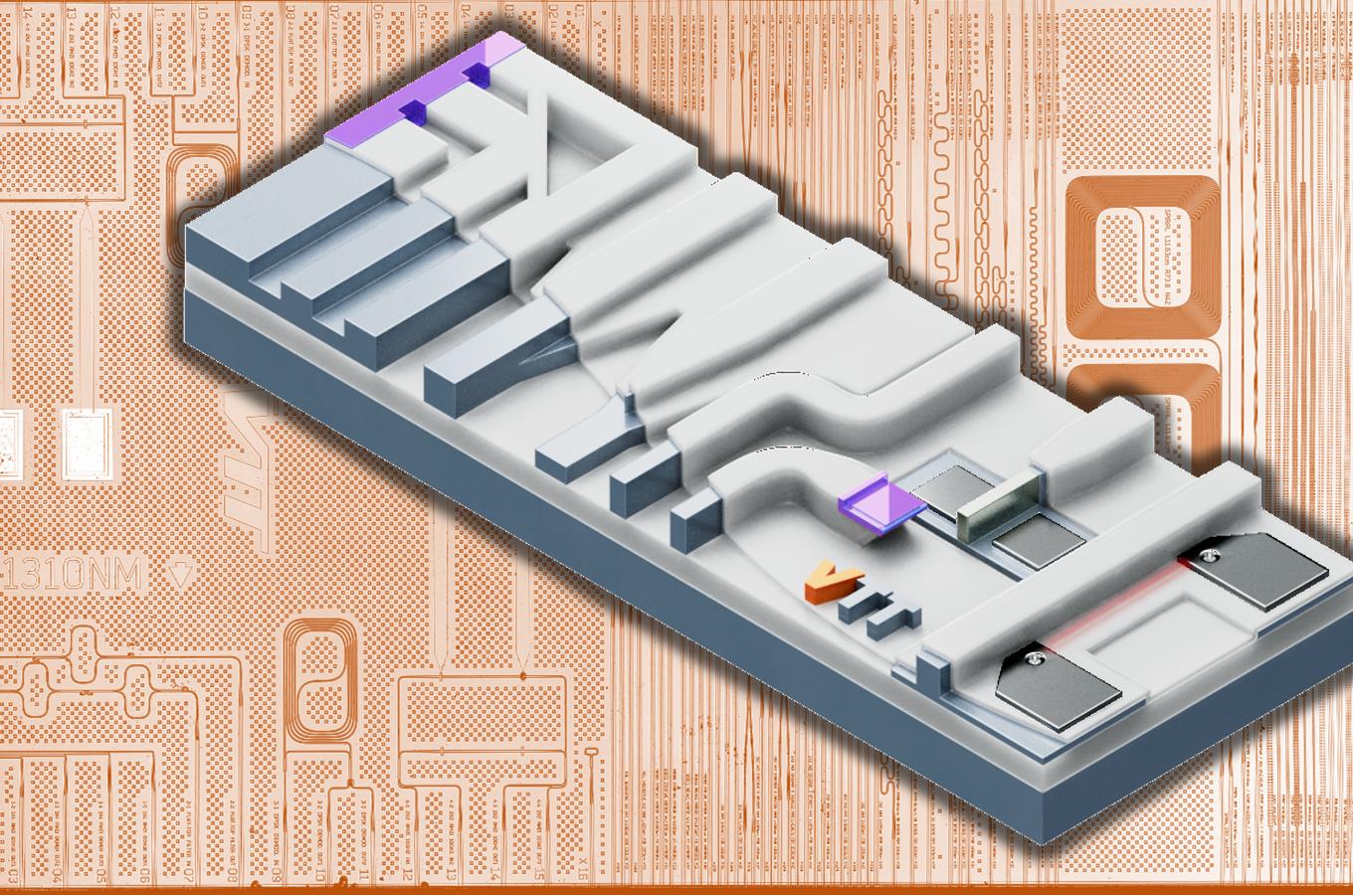
VTT finds Okmetic E-SOI® wafers highly beneficial platform for its Photonics Technology

Silicon wafer manufacturer Okmetic invests nearly 400 million euros to build a new fab in Finland with aims to more than double the production capacity and business

The Social Responsibility Report for 2021 has been published

Okmetic sponsoring and speaking at the CMC Conference on 27-29 April

  • Previous
  • 1
  • 2
  • 3
  • 4
  • 5
  • 6
  • 7
  • 8
  • Next
  • Silicon Wafers
    • Column
      • SOI Wafers – Silicon-On-Insulator Line
      • Patterned Wafers – DRIE and Lithography
      • TSV Wafers – Through Silicon Via
    • Column
      • RFSi® Wafers – High Resistivity Line for RF
      • SSP Wafers – Single Side Polished
      • DSP Wafers – Double Side Polished
    • Column
      • Power wafer line
      • Customized Wafers and Prototyping
      • Production and Subcontracting
To front page
  • About Okmetic
  • Contact Us
  • Applications
  • Quality and Responsibility
  • Work with Us
  • Privacy Policy and Terms of Use
  • Safety Data Sheet
LinkedIn YouTube WeChat Facebook