Skip to content
To front page
  • Silicon Wafers
    • MEMS Wafer Line
      • MEMS SSP and DSP Wafers
      • Selecting the ideal wafer for MEMS devices: Balancing cost, performance, and manufacturing efficiency
    • RFSi® Wafer Line – High Resistivity for RF
      • High Resistivity Wafers
      • Engineered High Resistivity Wafers with Trap-Rich Layer
      • Engineered Ultra High Resistivity wafers
      • UF-RFSi® – Ultra Flat High Resistivity Wafers
      • High Resistivity BSOI Wafers
      • RF GaN Substrate wafers
      • White paper “Advancing from 4G LTE to 5G and 6G: Engineered RFSi® Silicon Wafers for High-Performance RF Devices”
    • Power Wafer Line
      • Power Management SOI wafers
      • Power GaN Substrate wafers (Si and SOI) 
      • Discrete Power Device wafers 
      • White paper: “Enabling next-gen power and RF GaN devices with optimized silicon and SOI substrates” 
    • SOI Wafers – Silicon-On-Insulator Line
      • BSOI Wafers – Bonded SOI
      • C-SOI® Wafers – Cavity SOI
      • E-SOI® Wafers – Enhanced SOI
      • Terrace Free SOI wafers
    • Patterned Wafers – DRIE and Lithography
    • TSV Wafers – Through Silicon Via
    • DSP Wafers – Double Side Polished
    • SSP Wafers – Single Side Polished
    • Customized Wafers and Prototyping
    • Production and Capacity Expansion 
    • Supplier Awards and Collaboration Projects
  • Applications
    • MEMS and Sensors
    • RF Filters and Devices
    • Power Devices
  • Quality
    • Certificates
    • Quality Policy
    • Quality Tools
      • Artificial Intelligence at Okmetic
      • 5S at Okmetic
  • Sustainability
    • Environment and Targets
    • Responsibility for Personnel
    • Responsibility for Health and Safety
    • Business Ethics
    • Managing Responsibility
    • Sustainability Report and Certificates
  • Work with Us
    • Production Experts
    • Semiconductor Professionals
    • Students
    • Maintenance professional
    • Technical professionals
    • Sales and technical support
    • Open Positions
  • About Okmetic
    • Company
    • Strategy and Values
    • Executive Management Group
    • Investments
    • Research and Development Work
    • Tale of a Silicon Wafer
    • The History of Okmetic
    • News & Insights
    • Contact Us
  • English
    • Suomi
    • 日本語
    • 中文 (中国)

News

Okmetic+About Okmetic+News & insights+News

Select content category

  • Display all
  • Career stories
  • Events
  • Insights
  • Product news

Product Release: Okmetic Expands Its RFSi™ Portfolio with Tailored Silicon Substrate for Thin Film Surface Acoustic Wave Hybrid Structures

Okmetic recertified to conform to IATF 16949:2016 standards

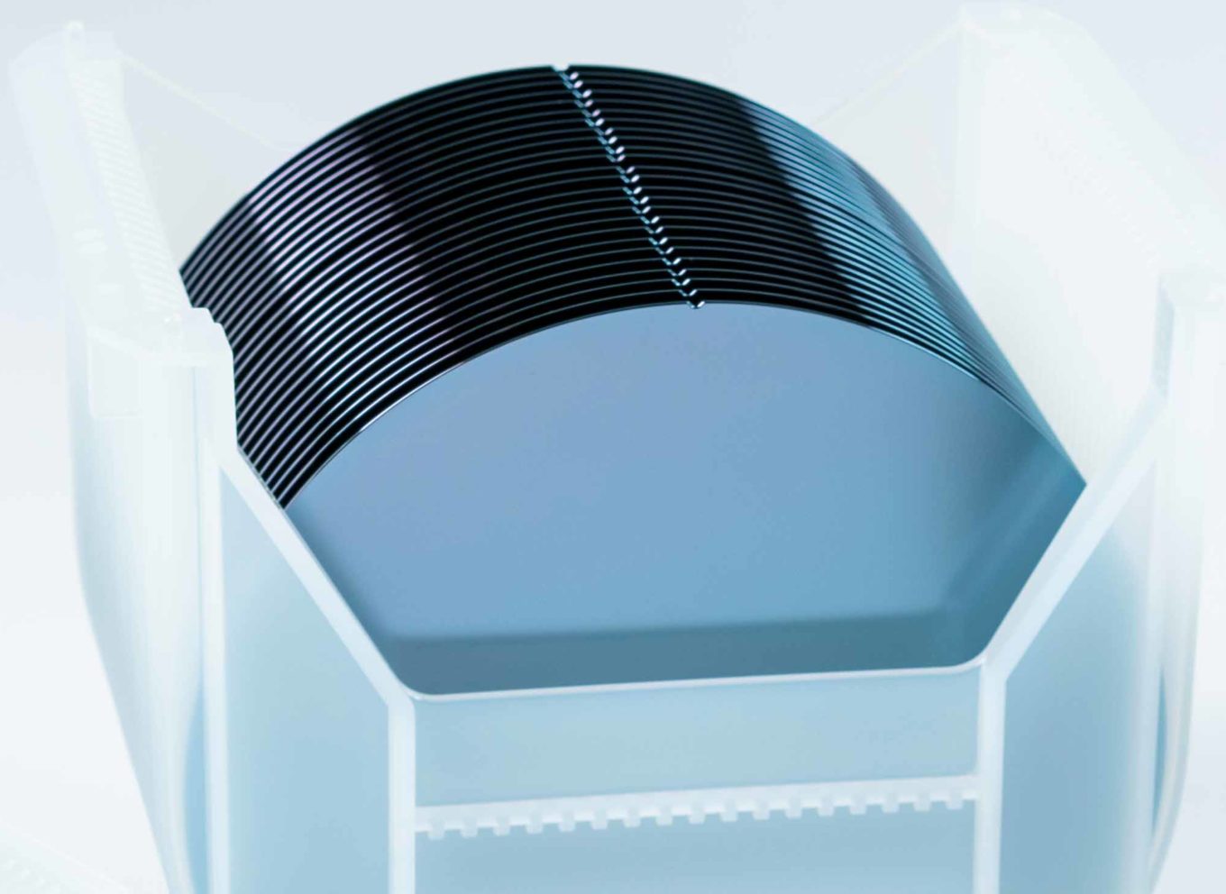
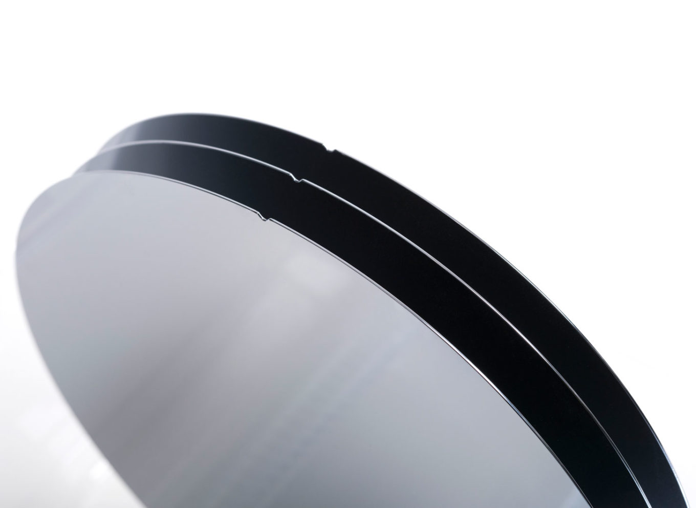
New MEMS silicon substrate standard helps everyone in the industry – Okmetic greatly involved in SEMI Manufacturing Working Group’s standardization and guideline work

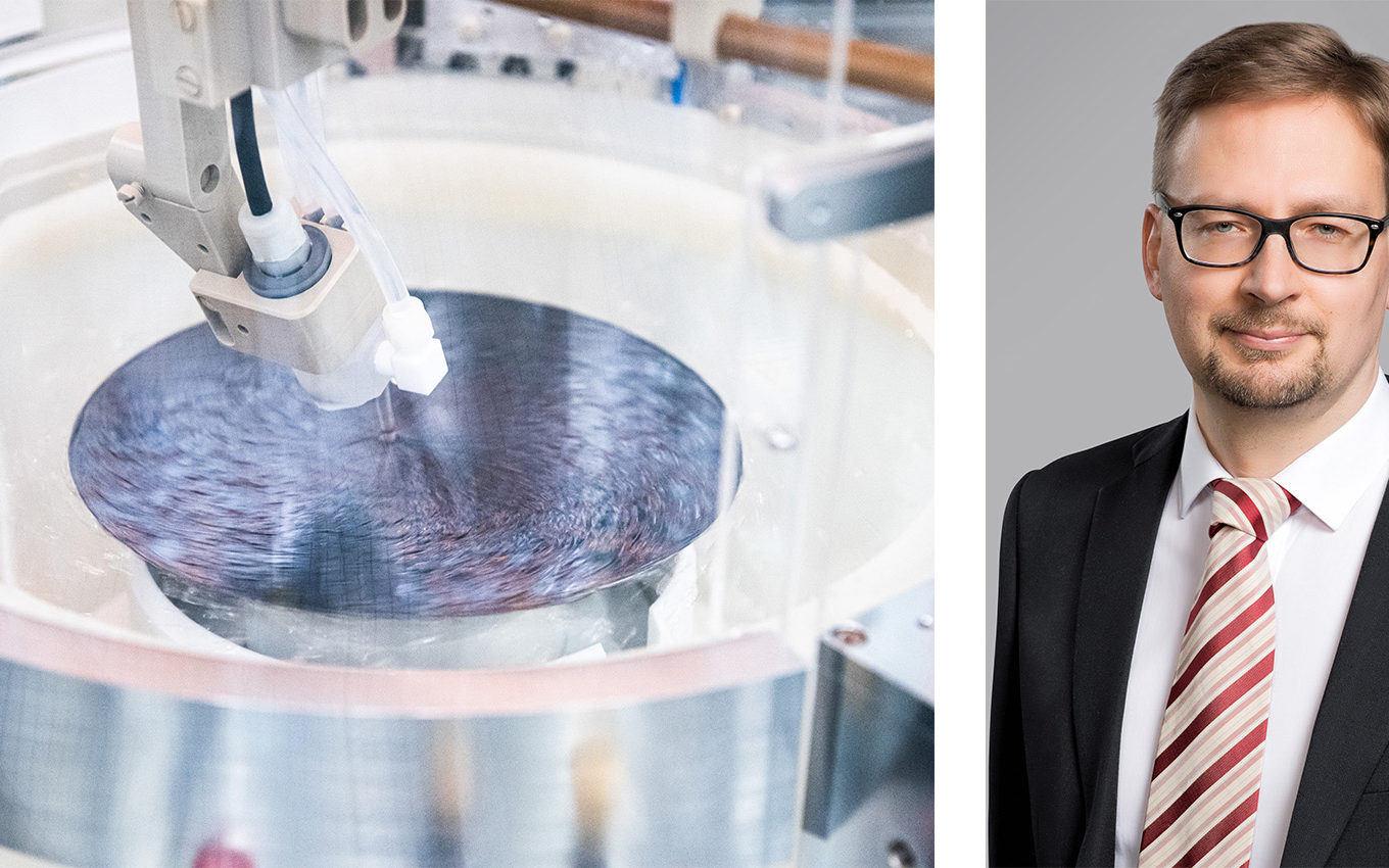
Okmetic’s Petri Santala is speaking in MSIG’s upcoming webinar on MEMS substrates evolution and standards

Okmetic appoints Vesa-Pekka Lempinen Chief Quality Officer making quality the highest priority

Okmetic news

Dr. Tzu-Yin Chiu appointed as NSIG’s President

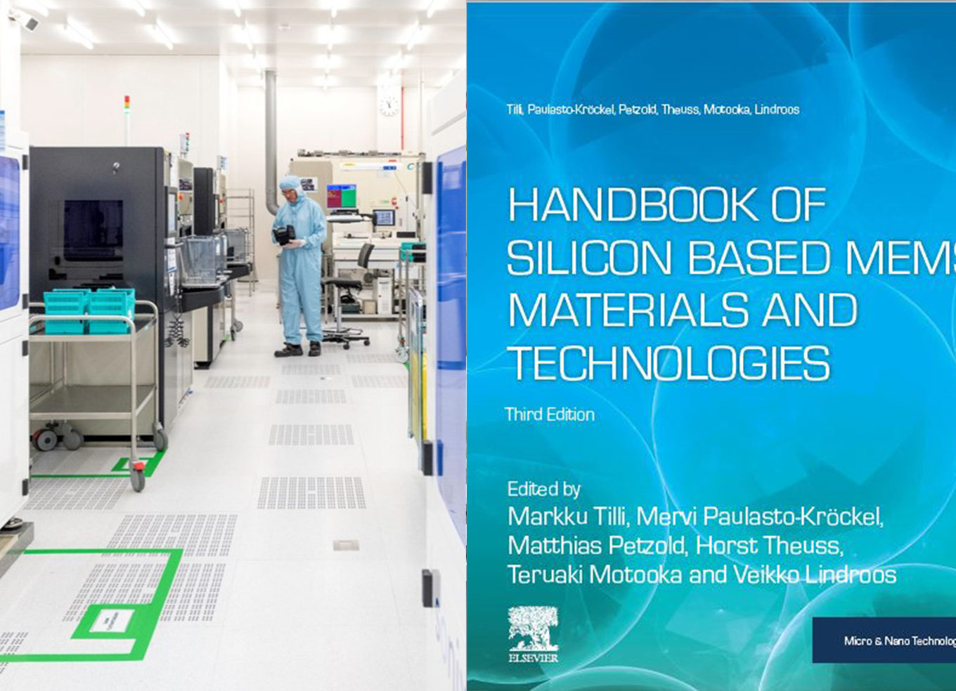
The long-awaited third edition of Handbook of Silicon Based MEMS Materials and Technologies is out now

Okmetic’s parent company NSIG listed on the SSE STAR market

Okmetic’s operations are stable despite globally worsening COVID-19 situation

Okmetic’s production running normally

Okmetic is making efforts to minimize COVID-19’s effect on its operations

Anna-Riikka Vuorikari-Antikainen appointed CCO

Okmetic’s Anna-Riikka Vuorikari-Antikainen elected as SMG’s Vice Chairman

Okmetic news

Päivi Sievilä’s presentation is the winner of MEMS & Imaging Sensors’ Technology Showcase

Okmetic news

Okmetic invests in high-performance wafers to enhance MEMS and sensor capabilities

  • Previous
  • 1
  • 2
  • …
  • 4
  • 5
  • 6
  • 7
  • 8
  • Next
  • Silicon Wafers
    • Column
      • SOI Wafers – Silicon-On-Insulator Line
      • Patterned Wafers – DRIE and Lithography
      • TSV Wafers – Through Silicon Via
    • Column
      • RFSi® Wafers – High Resistivity Line for RF
      • SSP Wafers – Single Side Polished
      • DSP Wafers – Double Side Polished
    • Column
      • Power wafer line
      • Customized Wafers and Prototyping
      • Production and Subcontracting
To front page
  • About Okmetic
  • Contact Us
  • Applications
  • Quality and Responsibility
  • Work with Us
  • Privacy Policy and Terms of Use
  • Safety Data Sheet
LinkedIn YouTube WeChat Facebook